

Semiconductor device having one of patterned SOI and SON structure
a semiconductor and son technology, applied in semiconductor devices, semiconductor/solid-state device details, electrical apparatus, etc., can solve the problems of change in electron or hole mobility, unsuitable circuit for mos transistor formed on an soi,
- Summary
- Abstract
- Description
- Claims
- Application Information
AI Technical Summary
Benefits of technology
Problems solved by technology
Method used
Image

Examples
first embodiment
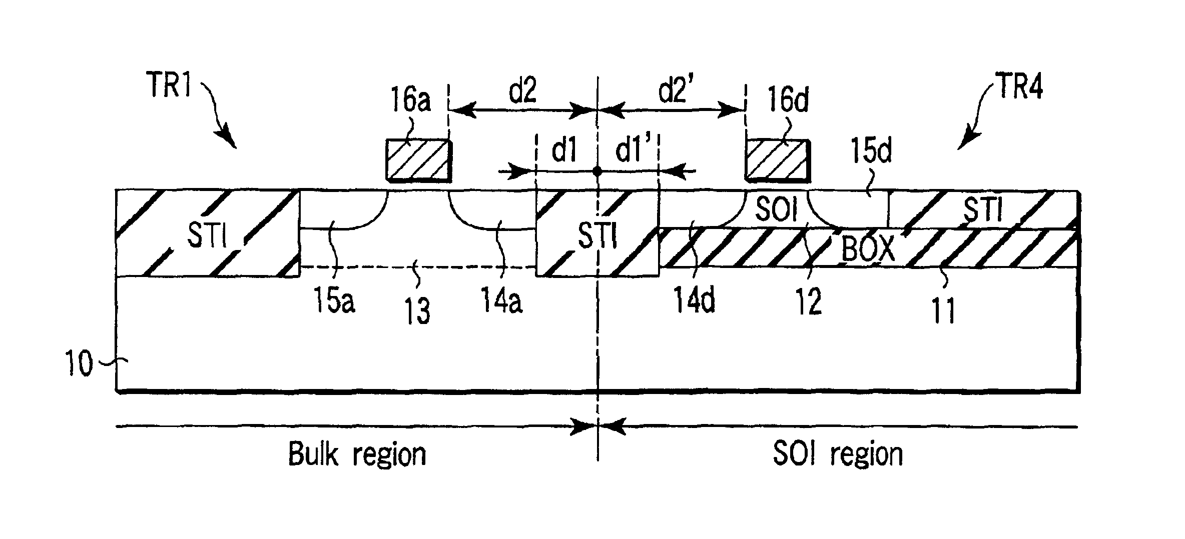
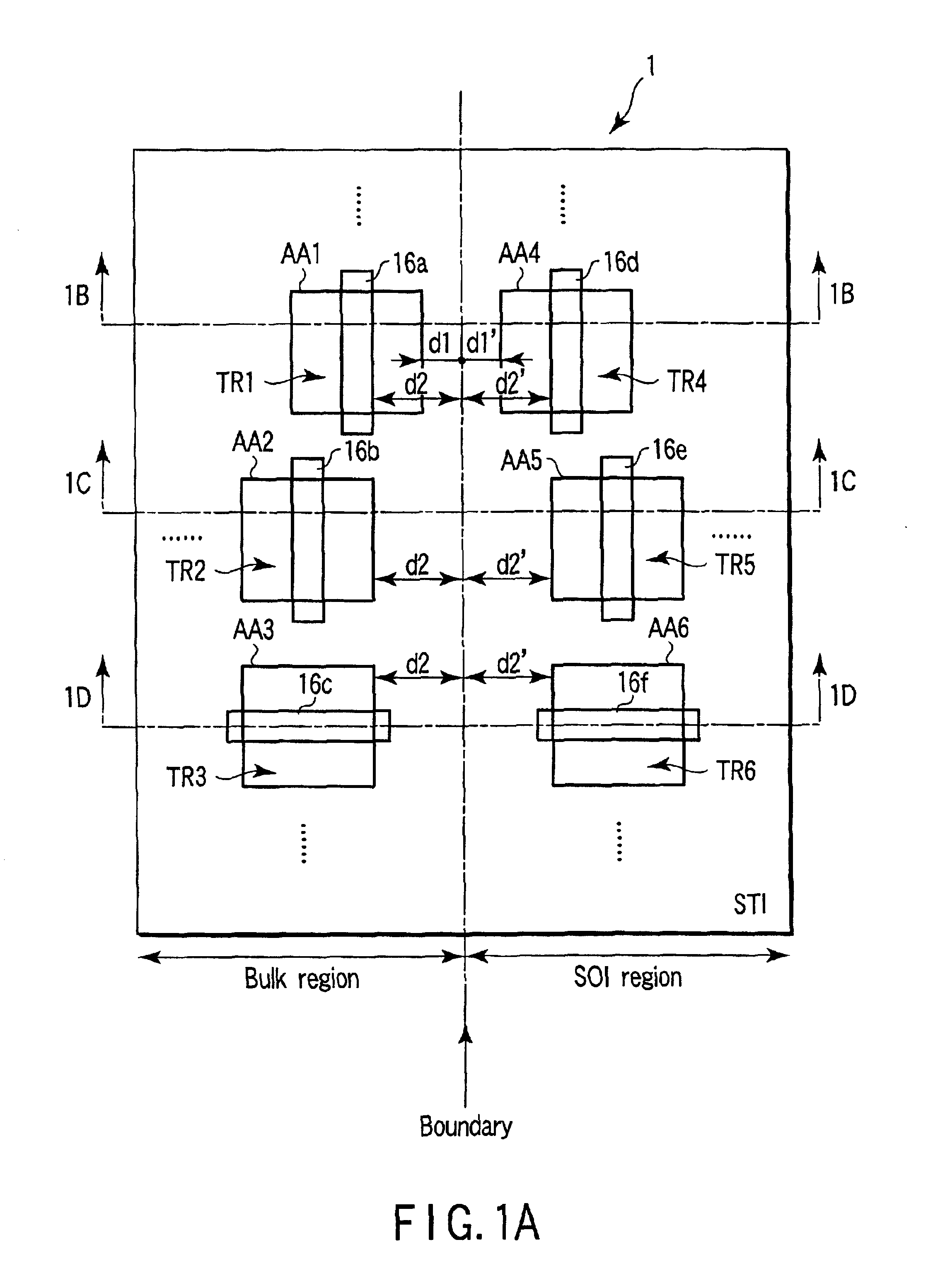
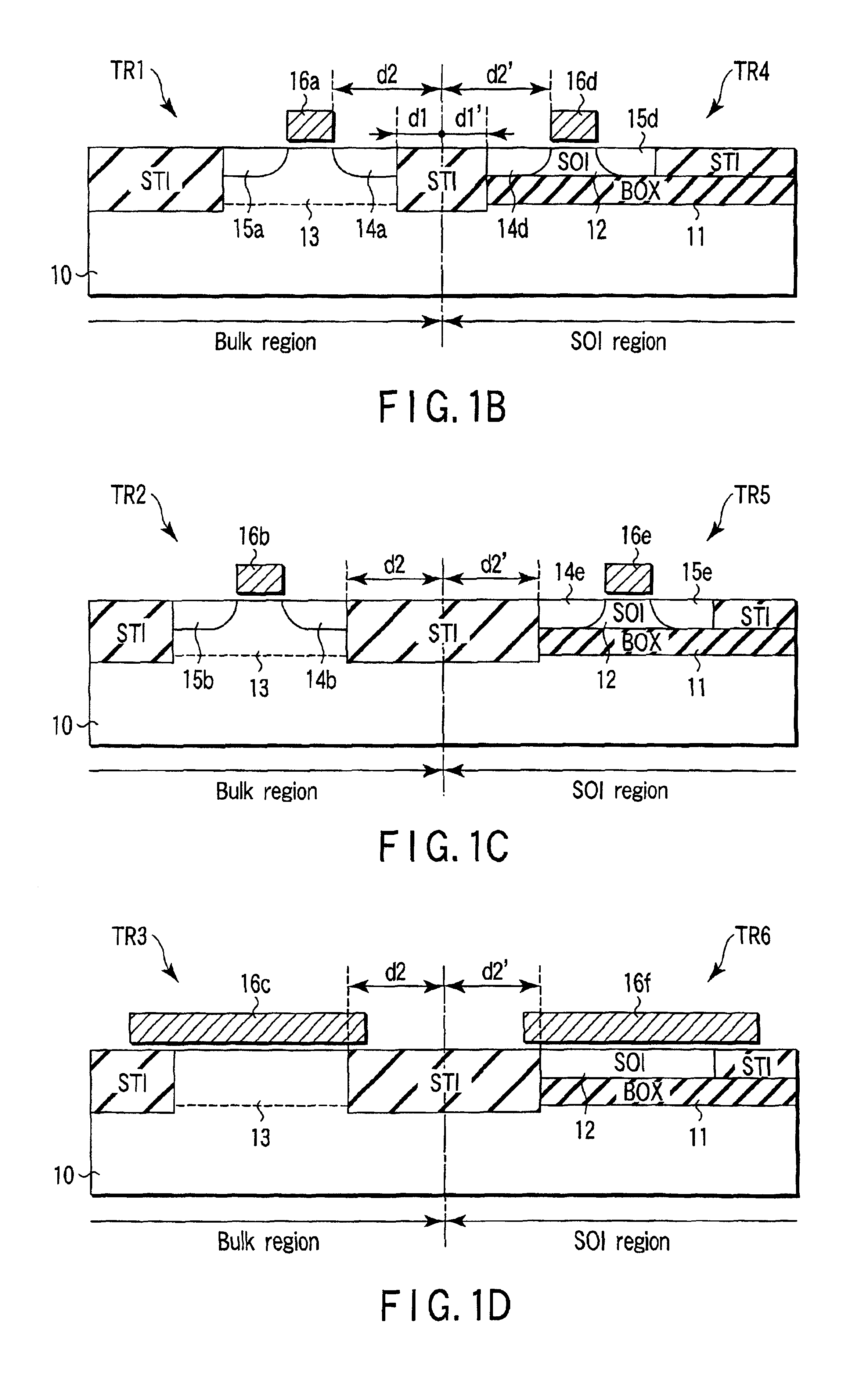
[0032]A semiconductor device according to the present invention will be described with reference to FIG. 1A. FIG. 1A is a plan view of a semiconductor device having a patterned SOI structure.
[0033]As illustrated in FIG. 1A, the semiconductor device 1 has a bulk region and an SOI region. The bulk region and the SOI region include element regions AA1 to AA6, which are electrically isolated from one another by element isolating regions STI. The element regions AA1 to AA6 respectively include MOS transistors TR1 to TR6. The MOS transistors TR1 to TR6 respectively have gate electrodes 16a to 16f. The gate electrodes 16a, 16b, 16d and 16e of the MOS transistors TR1, TR2, TR4 and TR5 extend parallel to the boundary between the bulk region and the SOI region. The gate electrodes 16c and 16f of the MOS transistor TR3 and TR6 extend perpendicular to the boundary.
[0034]The element region AA1 is located at a predetermined distance d1 from the boundary. The element regions AA2 and AA3 are locate...
third embodiment
[0064]A semiconductor device according to the present invention will now be described with reference to FIG. 8A. FIG. 8A is a plan view of a system LSI embedded a DRAM using a patterned SOI structure.
[0065]As illustrated in FIG. 8A, a DRAM cell array is formed in a bulk region of the patterned SOI structure as in the first and second embodiments, and a logic circuit is formed in the SOI region. A DRAM cell dummy pattern is formed in the boundary portion between the bulk region and the SOI region.
[0066]FIG. 8B is an enlarged view of a region B6 in FIG. 8A. As illustrated, a plurality of element regions AA are arranged in a staggered manner in the bulk region. The diagonally shaded portions in FIG. 8B represent the element regions AA. The element regions AA are surrounded by element isolating regions STI. Each element region has a length 5F (F is a minimum processing dimension) in the longitudinal direction and a length 1F in the direction perpendicular to the longitudinal direction. ...
PUM
 Abstract
Description
Claims
Application Information