Inspection of surfaces

a technology for inspecting surfaces and surfaces, applied in the direction of microscopes, optical elements, instruments, etc., can solve the problems of insufficient resolution of conductor tracks, time-consuming measurement, and insufficient fineness of resolution for microstructures with conductor tracks, so as to improve the measurement of contamination or damage on surfaces.

Inactive Publication Date: 2005-06-14
KONINKLIJKE PHILIPS ELECTRONICS NV
View PDF7 Cites 2 Cited by
  • Summary
  • Abstract
  • Description
  • Claims
  • Application Information

AI Technical Summary

Benefits of technology

[0003]It is an object of the invention to enhance the

Problems solved by technology

Such a resolution, however, is not fine enough for the microstructures with conductor tracks or component grou

Method used


Image

  • Inspection of surfaces
  • Inspection of surfaces
  • Inspection of surfaces

Examples


Embodiment Construction

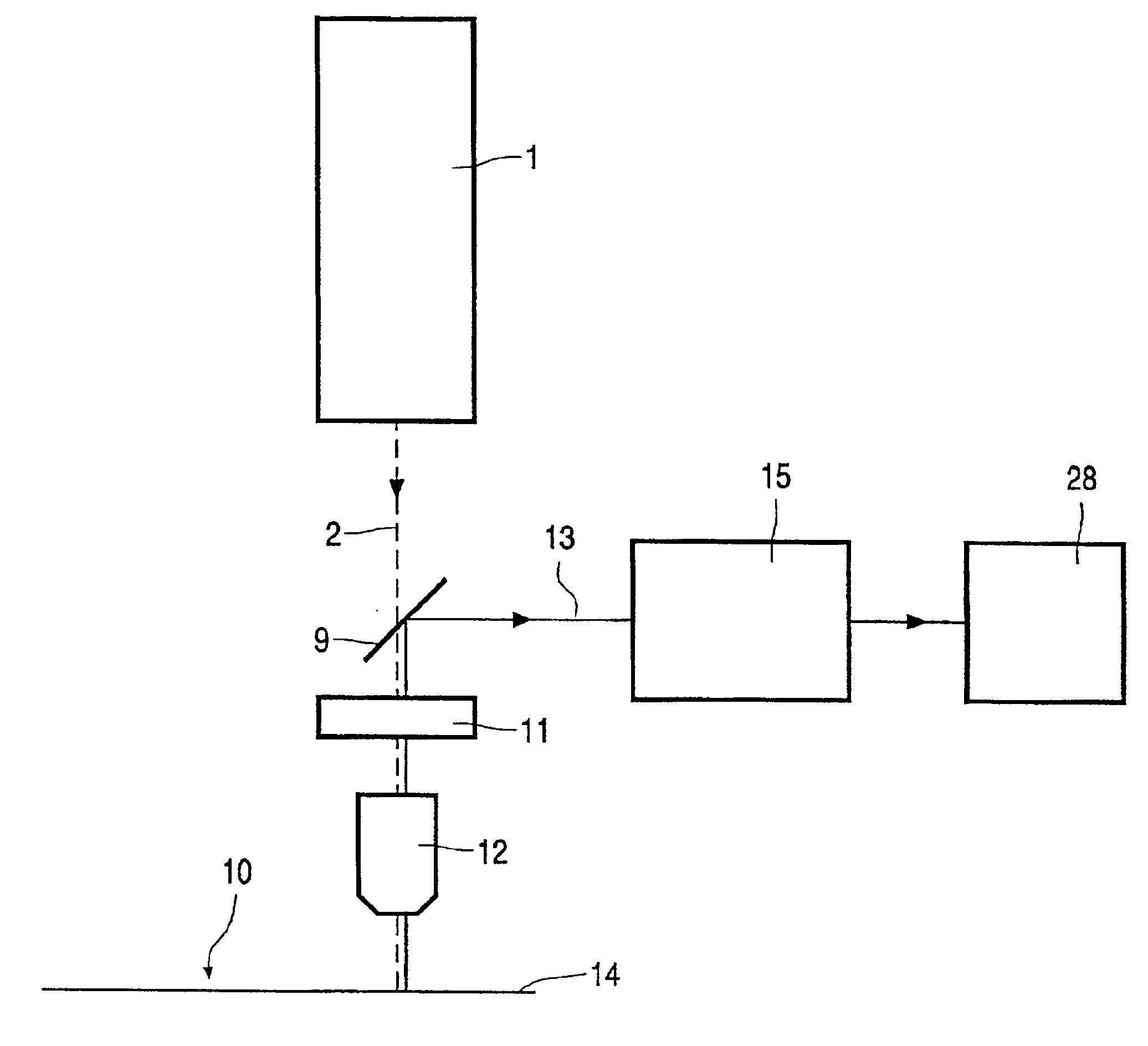
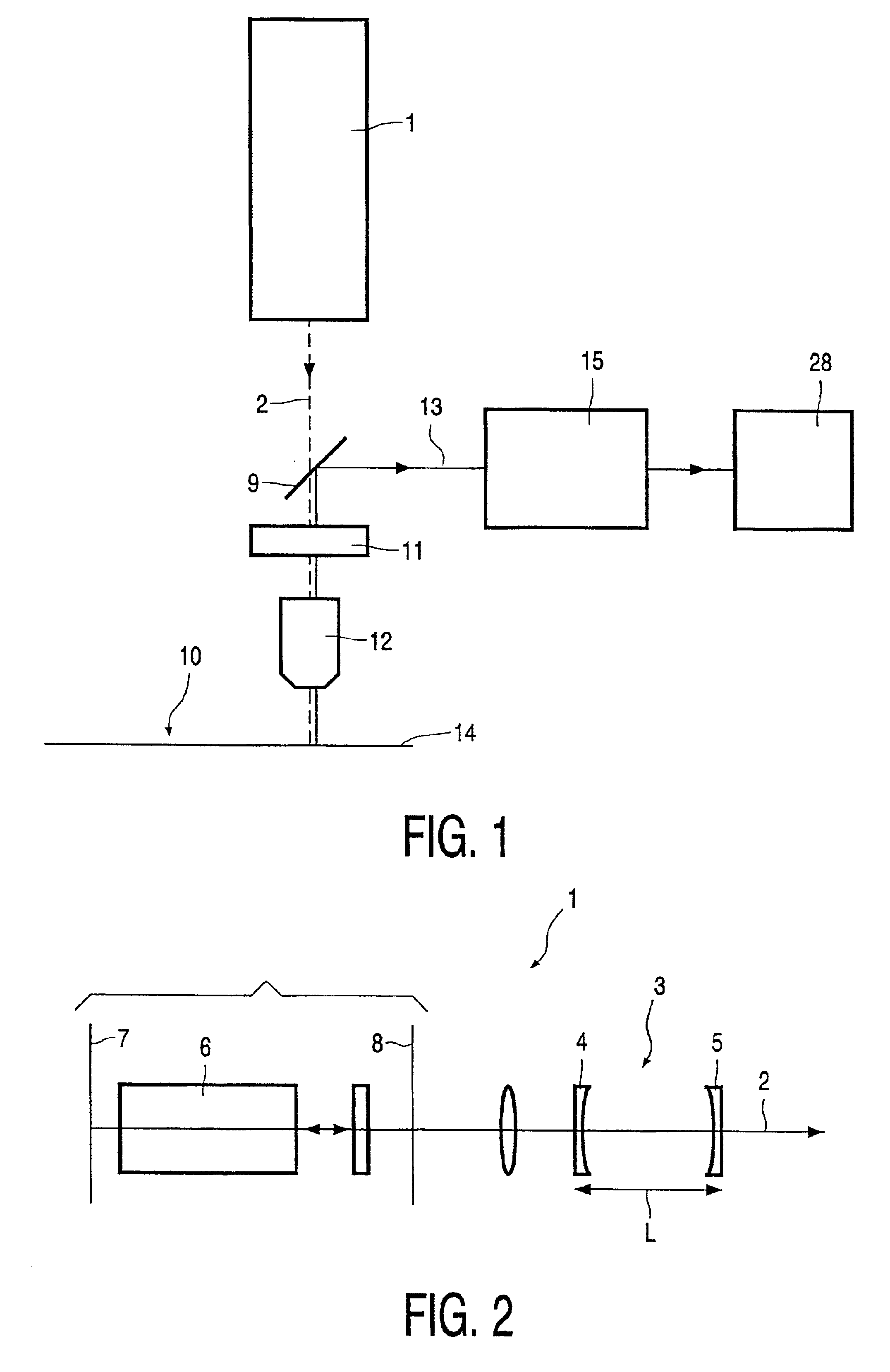
[0018]The embodiment of the device that is shown in FIG. 1 includes a light source 1 which is constructed as a laser light source and hence produces a high intensity. The laser light source 1 is provided with an optical resonator 3 which includes, for example mirrors 4, 5 that are adjustable relative to one another and are situated at a distance L from one another in the beam path of an emitted light beam 2. The mirrors 4, 5 are constructed as plane mirrors or as concave mirrors for ease of adjustment. Between these mirrors a standing wave is formed when the resonance condition is satisfied; this standing wave can be classified as a TEMmnp, where the term TEM stands for transversal electromagnetic moment and the index m denotes the number of zero positions in the x direction, n is the number of zero positions in the y direction and p is the number of nodes along the length L of the resonator axis (of the order of magnitude of 106 in the case of visible light and when the resonator h...


PUM


Abstract

A device for the inspection of surfaces, notably for the inspection of a surface of a semiconductor (14), which device comprises at least one laser light source (1) and a detector for detecting the light (13) that is reflected from the surface (10) to be inspected; the device also includes at least one mode filter (15; 15.1) for filtering the reflected light.

Description

FIELD AND BACKGROUND OF THE INVENTION[0001]The invention relates to a device for the inspection of surfaces as disclosed in the introductory part of claim 1, as well as to a mode filter as disclosed in the introductory part of claim 7, and to a method for the inspection of surfaces as disclosed in the introductory part of claim 9.[0002]WO 97 / 34123 teaches the use of a laser for the inspection of surfaces where the light reflected by the surface is detected. When a defect occurs in or on the surface, the light applied to the surface by the laser light source is reflected in such a manner that at least a part of the light is scattered by the defect. The intensity thus decreases in the reflected component. Therefore, localization of defects is possible by measurement of the intensity of the reflected light. The resolution is limited and amounts to approximately 500 nm. Such a resolution, however, is not fine enough for the microstructures with conductor tracks or component groups that ...

Claims


Application Information

Patent Timeline
IPC IPC(8): G01N21/88G01N21/95
CPCG02B21/0016G01N21/9501
Inventor HENDRIKS, ROBERT FRANS MARIATUKKER, TEUNIS WILLEM
Owner KONINKLIJKE PHILIPS ELECTRONICS NV
Why Eureka
Try Eureka