
Packet processing device

a processing device and packet technology, applied in data switching networks, frequency-division multiplexes, instruments, etc., can solve the problems of os protocol processing speed, memory copy which takes a long processing time, and large overhead, so as to reduce the number of processing of receiving packets and eliminate the overhead of os

Inactive Publication Date: 2005-06-14
FUJITSU LTD
View PDF11 Cites 230 Cited by
  • Summary
  • Abstract
  • Description
  • Claims
  • Application Information

AI Technical Summary

Benefits of technology

[0067]It is an object, of the present invention to provide a packet processing device which realizes a layered communication protocol processing wherein a packet processing is sped up without influences between processes in each layer.

Problems solved by technology

As a result, the memory copy which takes a long processing time in the protocol processing within the OS becomes unnecessary and the OS protocol processing is sped up.
In this case, since the OS is interrupted every time the NIC device receives a packet for the packet processing, it has a big overhead.
However, since a lower layer OS within the network interface performs an ordinary packet reception, from the viewpoint of packet forwarding by the hardware, the hardware processing is blocked when the number of the received packets increases.
While this L3 switch performs the network layer packet forwarding processed by a high-speed hardware, the memory access from the OS causes the packet forwarding of the hardware to be blocked and degrades the routing performance.
(1) Since this is devised by assuming the filtering and the policy setting which may be achieved by the hardware of the L3 switch, a complex session identification or the like requires a software processing.
(2) Since the hardware processing for the traffic via an application cannot be performed by the L3 switch, an application gateways which looks into the contents of a packet cannot achieve a satisfactory performance.

Method used


Image

  • Packet processing device
  • Packet processing device
  • Packet processing device

Examples


Embodiment Construction

[0134]FIG. 4 shows an embodiment (1) of the packet processing device 10 according to the present invention, wherein the packet processing device 10 is composed of an interface module 30 for transferring a transmitting packet 95 and a receiving packet 90 to / from a network, an OS kernel 20 for transferring the packets to / from the module 30, and an application layer protocol processor (synonymous with “application program” and “application”) 11 operating on the OS kernel 20.

[0135]The interface module 30 is composed of a receiving interface 31 for receiving the packets, a connection identifying circuit 32, a checksum calculating circuit 33, a header deleting circuit 34, a reassembly buffer writing circuit 35, a reassembly buffer 36, a buffer control circuit 37, a buffer condition determining circuit 38, a timer 39, a receiving queue 40, a DMA transfer circuit 41, a connection queue 42, a service list 43, a transmitting queue 44, a transmitting buffer 45, and a transmitting interface 46 ...


PUM


Abstract

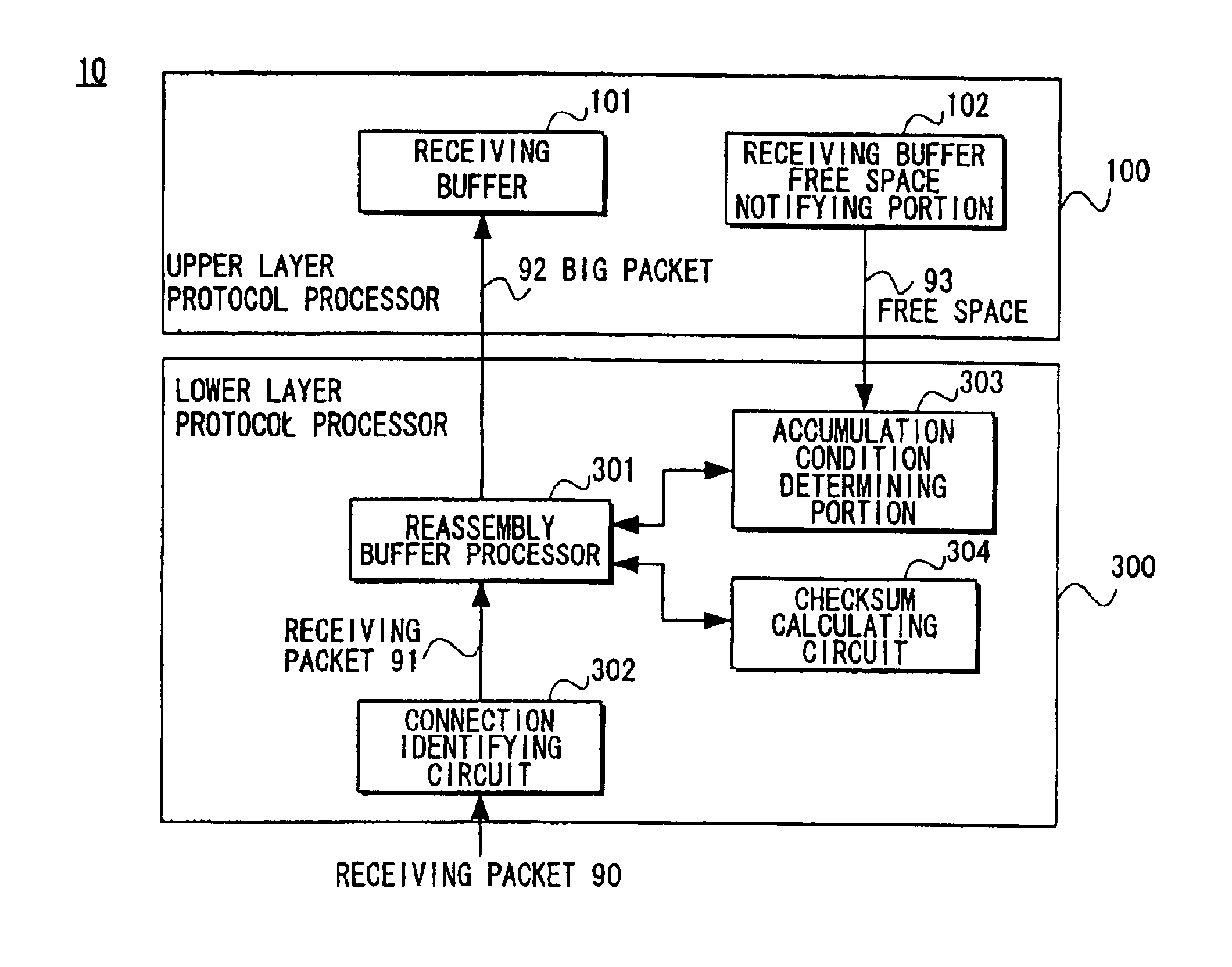
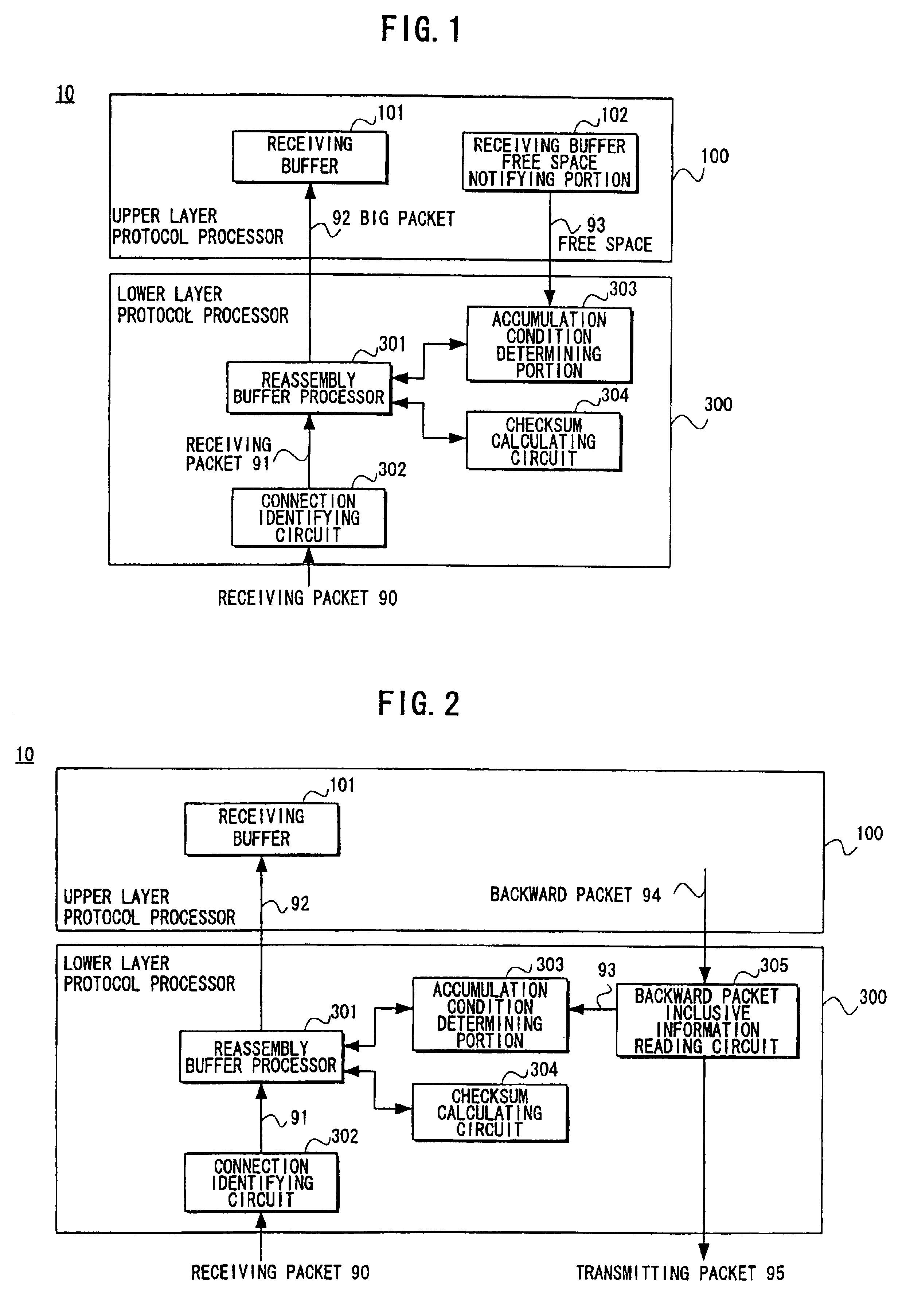
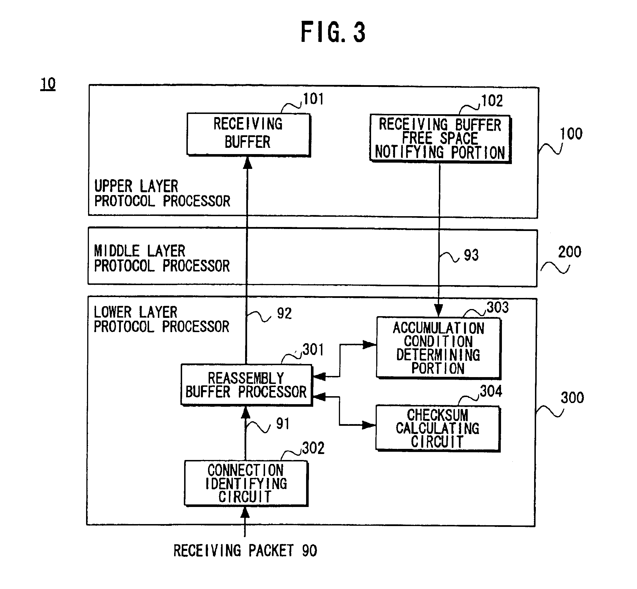
A packet processing device in which a receiving buffer free space notifying portion notifies a free space of a receiving buffer, an accumulation condition determining portion determines a size of a big packet based on the free space, and a reassembly buffer processor reassembles a plurality of receiving packets into a single big packet to be transmitted to the receiving buffer. A backward packet inclusive information reading circuit for detecting the free space based on information within a backward packet from the upper layer may be used as the receiving buffer free space notifying portion. Also, an application layer may be used as the upper layer so that the big packet is transmitted not through a buffer of a transport layer but directly to the receiving buffer.

Description

BACKGROUND OF THE INVENTION[0001]1. Field of the Invention[0002]The present invention relates to a packet processing device, and in particular to a packet processing device which has a layered communication protocol.[0003]In recent years, a packet processing device which has a hierarchically structured communication protocol such as a TCP / UDP / IP has been popularized as used in a router, a layer 3 (third layer) switch (hereinafter abbreviated as “L3 switch”) which performs a packet processing of a network layer on a hardware, a network interface device (Network Interface Card: hereinafter abbreviated as “NIC device”) of host systems, and the like.[0004]Also, as the communication technology in recent years has remarkably progressed, the transmission speed has become increased more and more. As a result, the packet processing device is required to follow up the speed.[0005]2. Description of the Related Art[0006]Having a main function of relaying packets in a network layer, the router a...

Claims


Application Information

Patent Timeline
IPC IPC(8): H04L29/08H04L12/56H04L47/36H04L47/43
CPCH04L47/30H04L69/32H04L49/90H04L49/9026H04L49/9094H04L49/602H04L49/3009H04L49/3018H04L49/351
Inventor OGUCHI, NAOKI
Owner FUJITSU LTD
Learn More