Method for fabricating encapsulated semiconductor components

a technology of semiconductor components and encapsulation, which is applied in the direction of semiconductor devices, semiconductor/solid-state device details, electrical devices, etc., can solve the problems of relative fragile semiconductor substrates that are susceptible to cracking and chipping, and achieve the effect of facilitating the testing of components

Inactive Publication Date: 2005-06-21
MICRON TECH INC
View PDF38 Cites 416 Cited by
  • Summary
  • Abstract
  • Description
  • Claims
  • Application Information

AI Technical Summary

Benefits of technology

[0011]The circuit side polymer layer is then formed on the bumps and in the trenches, and both the circuit side polymer layer and the bumps can be planarized. The circuit side polymer layer can be formed using a nozzle deposition process, a transfer molding process, an injection molding process, a screen printing process, a stenciling process, a spin resist process, a dry film process, a stereo lithographic process, or any other suitable deposition process. The circuit side polymer layer protects the dice during the fabrication process, and also protects the dice in the completed components. Following formation of the circuit side polymer layer, the substrate is thinned from the back side, such that the polymer filled trenches are exposed. The thinning step can be performed by mechanically planarizing the substrate or by etching the substrate.
[0012]Next, the back side polymer layer is formed on the thinned back side of the substrate and can also be planarized. The back side polymer layer can be formed as described above for the circuit side polymer layer. The back side polymer layer protects the dice during the fabrication process, and also protects the dice in the completed components.
[0013]Next, the terminal contacts are formed on the contact bumps using a suitable deposition or

Problems solved by technology

In this regard, semiconductor dice include relatively fragile semi

Method used


Image

  • Method for fabricating encapsulated semiconductor components
  • Method for fabricating encapsulated semiconductor components
  • Method for fabricating encapsulated semiconductor components

Examples


first embodiment

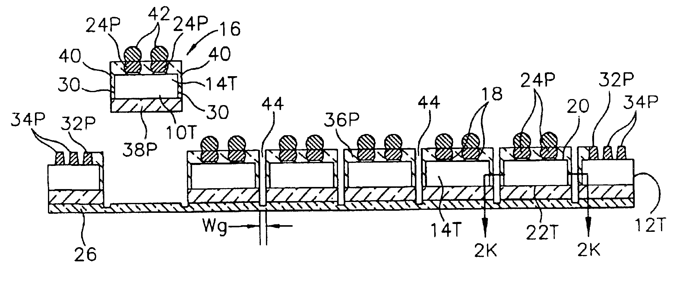
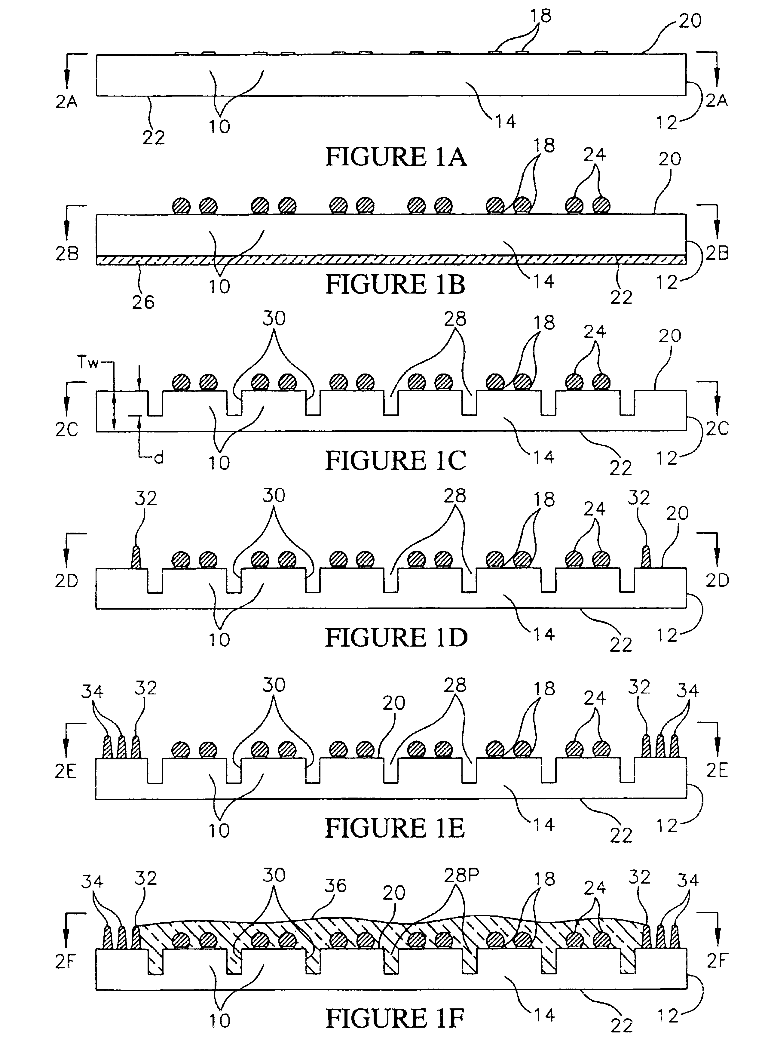
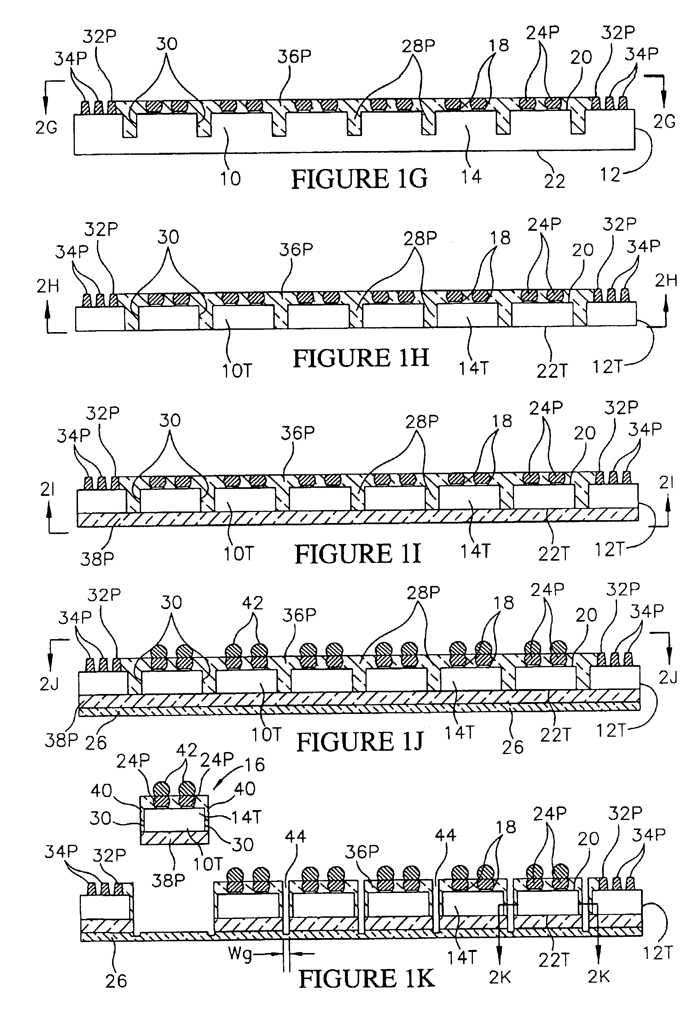
[0114]Referring to FIGS. 1A-1K, 2A-2K and 3A-3J, steps in the method for fabricating a first embodiment semiconductor component 16 (FIG. 1K) in accordance with the invention are illustrated. As will be further explained, each completed component 16 (FIG. 1K) contains a single die encapsulated by polymer layers on six surfaces. The component 16 is thus referred to as a “6X component”.

[0115]Initially, as shown in FIGS. 1A, 2A and 3A, a plurality of semiconductor dice 10 are provided, for fabricating a plurality of semiconductor components 16 (FIG. 1K). The dice 10 can comprise conventional semiconductor dice having a desired configuration. For example, each die 10 can comprise a dynamic random access memory (DRAM), a static random access memory (SRAM), a flash memory, a microprocessor, a digital signal processor (DSP) or an application specific integrated circuit (ASIC). The dice 10 and the components 16 can have any polygonal shape. In the illustrative embodiment, the dice 10 and the...

third embodiment

[0219]Referring to FIGS. 13A-13G, steps in a method for fabricating a third embodiment component 16E (FIG. 13F) are illustrated. In this embodiment, the components 16E (FIG. 13F) are singulated using an etching process. In addition, each component 16E (FIG. 13F) is hermetically sealed on five sides, such that a “15X component” is provided.

[0220]Initially, as shown in FIG. 13A, a plurality of semiconductor dice 10E are provided on a semiconductor wafer 12E, substantially as previously described. Each die 10E includes a semiconductor substrate 14E containing integrated circuits. In addition, the wafer 12E and each die 10E includes a circuit side 20E (first side) wherein the integrated circuits are located, and a back side 22E (second side). Each die 10E also includes a pattern of die contacts 18E on the circuit side 20E in electrical communication with the integrated circuits thereon. The die contacts 18E can be constructed like the previously described die contacts 18 in FIG. 1A, or ...

fourth embodiment

[0237]Referring to FIGS. 15A-15F, steps in a method for fabricating a fourth embodiment semiconductor component 16-1X (FIG. 15F) are illustrated. The semiconductor component 16-1X (FIG. 15F) contains a single semiconductor die 10-1X encapsulated on only the circuit side thereof, and is thus referred to as a 1X component.

[0238]Initially, as shown in FIG. 15A, a plurality of semiconductor dice 10-1X are provided on a semiconductor wafer 12-1X substantially as previously described. Each die 10-1X includes a semiconductor substrate 14-1X containing integrated circuits. In addition, the wafer 12-1X and each die 10-1X includes a circuit side 20-1X (first side) wherein the integrated circuits are located, and a back side 22-1X (second side). Each die 10-1X also includes a pattern of die contacts 18-1X such as redistribution pads or bond pads, on the circuit side 20-1X in electrical communication with the integrated circuits thereon.

[0239]Next, as shown in FIG. 15B, contact bumps 24-1X are ...


PUM


Abstract

A semiconductor component includes a thinned semiconductor die having protective polymer layers on up to six surfaces. The component also includes contact bumps on the die embedded in a circuit side polymer layer, and terminal contacts on the contact bumps in a dense area array. A method for fabricating the component includes the steps of providing a substrate containing multiple dice, forming trenches on the substrate proximate to peripheral edges of the dice, and depositing a polymer material into the trenches. In addition, the method includes the steps of planarizing the back side of the substrate to contact the polymer filled trenches, and cutting through the polymer trenches to singulate the components from the substrate. Prior to the singulating step the components can be tested and burned-in while they remain on the substrate.

Description

FIELD OF THE INVENTION[0001]This invention relates generally to semiconductor manufacture and packaging. More particularly, this invention relates to encapsulated semiconductor components, to methods for fabricating the components, and to systems incorporating the components.BACKGROUND OF THE INVENTION[0002]In semiconductor manufacture, different types of components have been developed recently, that are smaller and have a higher input / output capability than conventional plastic or ceramic packages. For example, one type of semiconductor component is referred to as a chip scale package (CSP) because it has an outline, or “footprint”, that is about the same as the outline of the die contained in the package.[0003]Typically, a chip scale package includes a dense area array of solder bumps, such as a standardized grid array as disclosed in U.S. Pat. No. 6,169,329 to Farnworth et al. The solder bumps permit the package to be flip chip mounted to a substrate, such as a package substrate,...

Claims


Application Information

Patent Timeline
IPC IPC(8): H01L21/60H01L23/28H01L23/31H01L23/49H01L21/68H01L21/02H01L21/70H01L21/768H01L21/67H01L23/485H01L23/48H01L23/367H01L23/34H01L21/301H01L21/304H01L21/44H01L21/56H01L21/78H01L23/24H01L23/495H01L29/06
CPCH01L21/3043H01L21/56H01L21/561H01L21/565H01L21/568H01L21/6835H01L21/6836H01L21/76802H01L21/76898H01L21/78H01L23/24H01L23/3114H01L23/36H01L23/481H01L23/49531H01L24/05H01L24/11H01L24/12H01L24/16H01L24/94H01L24/96H01L25/105H01L25/50H01L24/27H01L21/304H01L23/3672H01L23/49575H01L29/0657H01L2221/68327H01L2221/68331H01L2221/68372H01L2224/0401H01L2224/05599H01L2224/11901H01L2224/13009H01L2224/13022H01L2224/13025H01L2224/13099H01L2224/16H01L2224/274H01L2224/73253H01L2225/06541H01L2924/01002H01L2924/01004H01L2924/01005H01L2924/01013H01L2924/01014H01L2924/01015H01L2924/01022H01L2924/01028H01L2924/01029H01L2924/0103H01L2924/01039H01L2924/01042H01L2924/01046H01L2924/01047H01L2924/0105H01L2924/01073H01L2924/01074H01L2924/01075H01L2924/01077H01L2924/01078H01L2924/01079H01L2924/014H01L2924/05042H01L2924/12044H01L2924/14H01L2924/1433H01L2924/19041H01L2924/19042H01L2924/00013H01L2924/01006H01L2924/01019H01L2924/01033H01L2924/01041H01L2924/00014H01L2225/1035H01L2225/1058H01L2225/107H01L2225/1094H01L2224/12105H01L2224/16235H01L2924/3512H01L2924/00H01L2224/29099H01L2224/11849H01L2924/12042H01L2224/94H01L2224/73104H01L2224/04105B33Y80/00B33Y70/00H01L2224/023H01L2224/27H01L2924/0001H01L23/48
Inventor FARNWORTH, WARREN M.WOOD, ALAN G.DOAN, TRUNG TRI
Owner MICRON TECH INC
Why Eureka
Try Eureka