Method of forming tiny silicon nitride spacer for flash EPROM by fully wet etching technology

a technology of silicon nitride and spacer, which is applied in the field of split-gate memory cells, can solve the problems of difficult to control the dimensions, let alone the shape of the spacer, reverse tunneling, or erasing, and achieve the effect of shortening the manufacturing product cycl

Inactive Publication Date: 2005-06-21
TAIWAN SEMICON MFG CO LTD
View PDF15 Cites 1 Cited by
  • Summary
  • Abstract
  • Description
  • Claims
  • Application Information

AI Technical Summary

Benefits of technology

[0019]These objects are accomplished in a first embodiment where the main-etch and over-etch are accomplished using a recipe comprising a hot phosphoric acid (H3PO4) solution. In the second embodiment, phosphoric solution is used for main-etch only, while a Caro's-Sulfuric Peroxide solution (H2SO4+H2O2), or CR-SPM, is used as an over-etch in forming the tiny silicon nitride spacers of the invention. In the third embodiment, the step of over-etching of the spacers is combined with the step of stripping off of an implant photomask, thus, shortening the manufacturing product cycle.

Problems solved by technology

Especially when very small spacers are required for better performance of split-gate cells, a few seconds of etch time makes it very difficult to control the dimensions, let alone the shape of the spacers.
A poorly defined spacer will cause, what is known in the art as “write disturb”, or, unwanted reverse tunneling, or erasing.
Inadvertent reverse tunneling, or erasure, for example, may occur if the tunnel oxide is degraded, or the spacer formed between the floating gate and the control gate is poorly shaped.

Method used


Image

  • Method of forming tiny silicon nitride spacer for flash EPROM by fully wet etching technology
  • Method of forming tiny silicon nitride spacer for flash EPROM by fully wet etching technology
  • Method of forming tiny silicon nitride spacer for flash EPROM by fully wet etching technology

Examples


Embodiment Construction

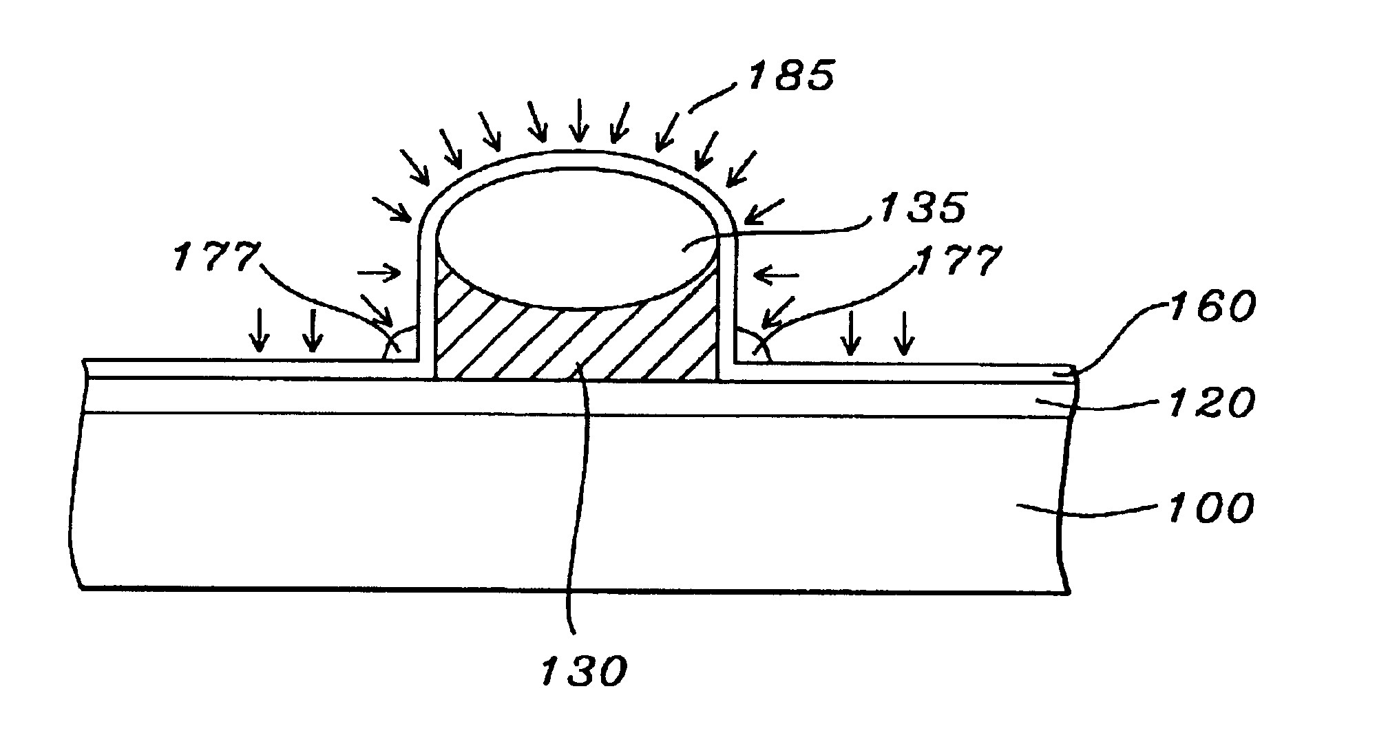
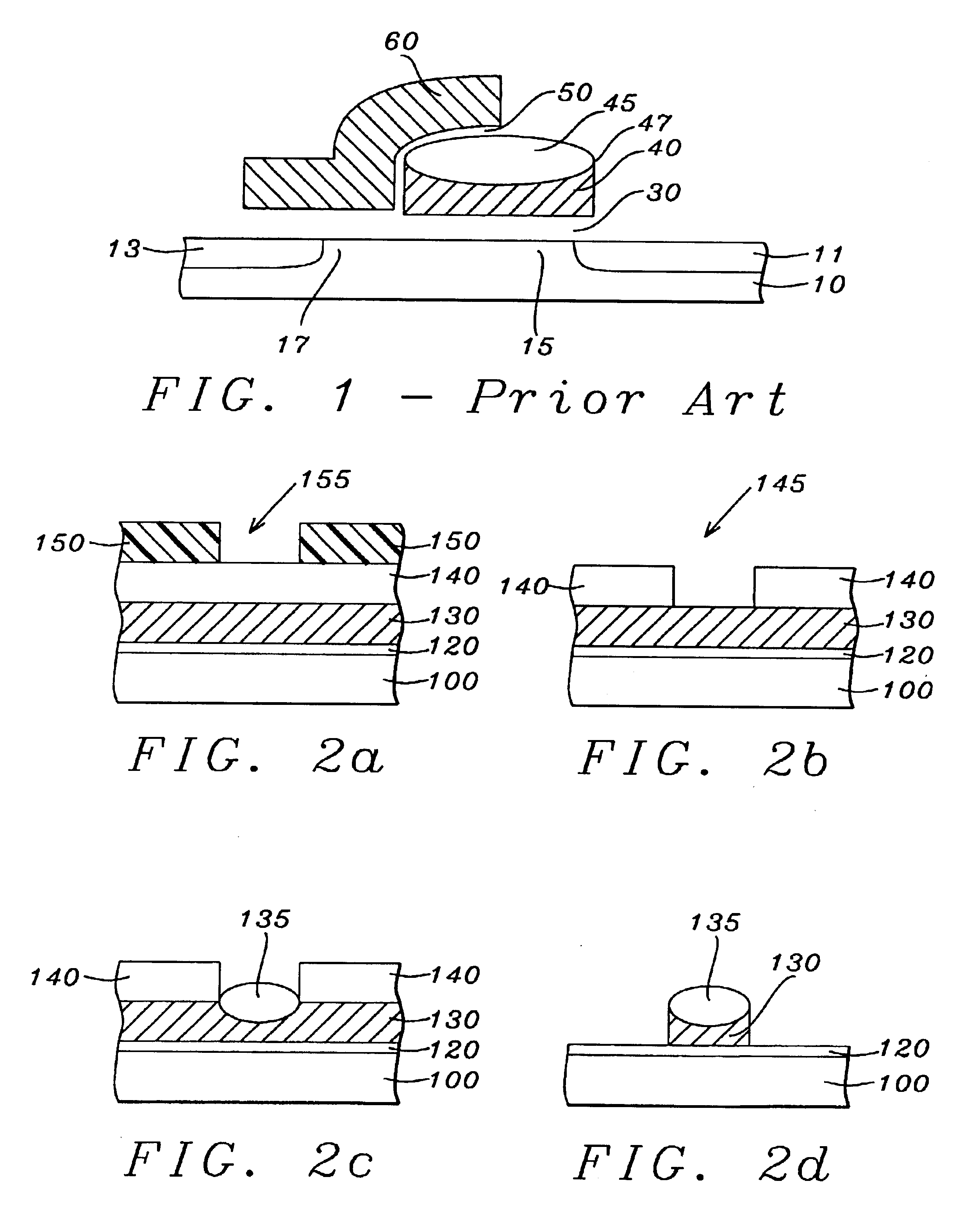
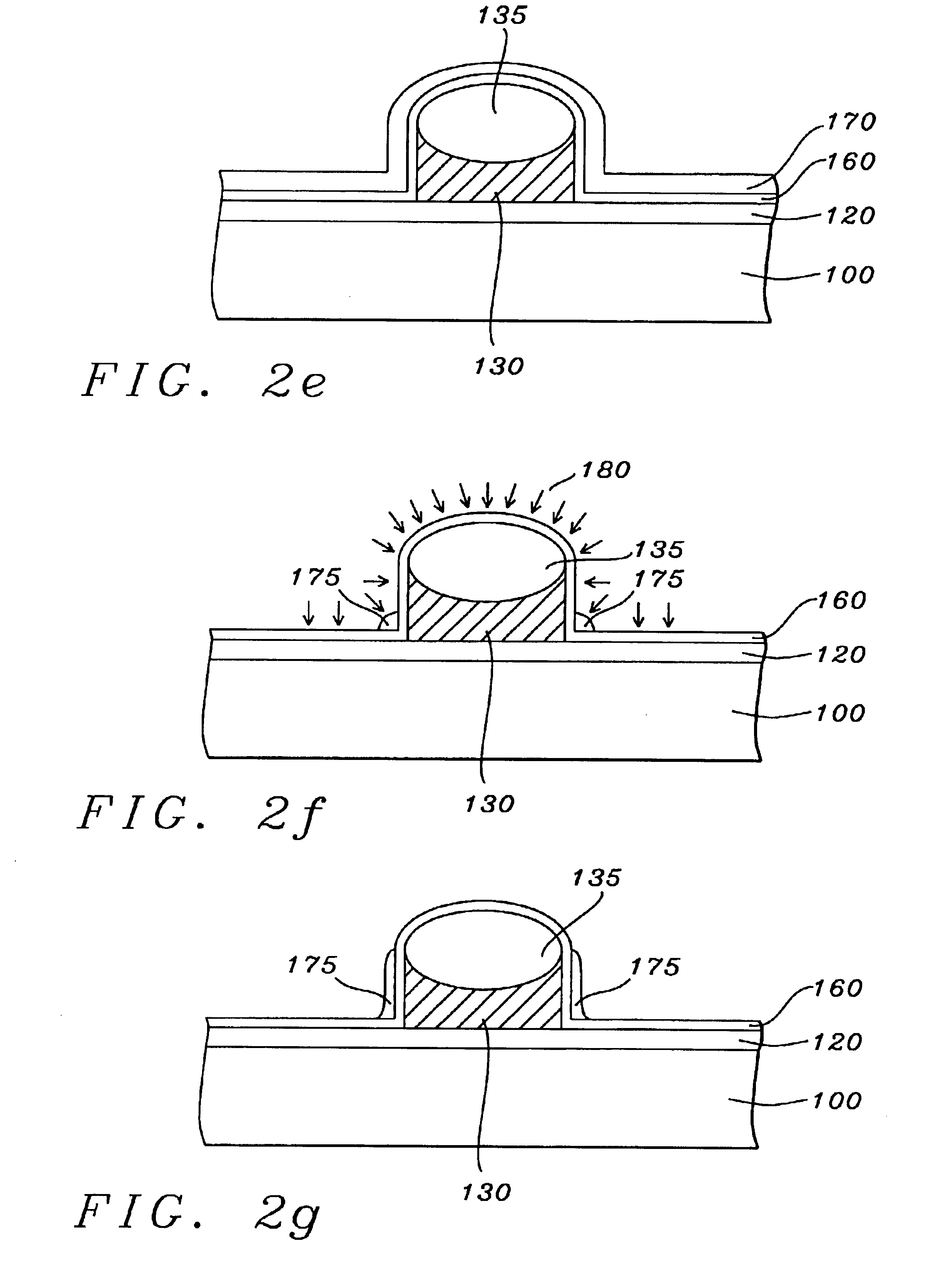
[0033]Referring now to the drawings, in particular to FIGS. 2a-2i, there is shown cross-sectional views of a substrate as the steps of the instant invention are practiced. The process steps are further summarized in Process Flow Charts in FIGS. 3a-3c. It will be appreciated by those skilled in the art that the fully isotropic wet etch method that is disclosed here is different from the conventional method of using only anisotropic dry etch method, and also different from a combination of dry anisotropic and wet isotropic methods practiced in the present manufacturing line. In contrast to the conventional only anisotropic dry etch methods, the isotropic fully wet etch method widens the conventional dry etch only process window (that is, process etch time) up to one hundred times or more so that the etching of very small dimensions can be controlled much more precisely. It is shown below in the embodiments of the present invention that a particular wet etch recipe must also be used in...


PUM

PropertyMeasurementUnit
voltageaaaaaaaaaa
voltageaaaaaaaaaa
temperatureaaaaaaaaaa

Abstract

A method of forming very small silicon nitride spacers in split-gate flash EPROMs is disclosed which prevent the occurrence of “write disturb”, unwanted reverse tunneling, or erasing. This is accomplished by forming spacers with well-controlled dimensions and well-defined shapes through a judicious use of a fully wet etch technique, including main-etch and over-etch. The use of a phosphoric acid solution in combination with sulfuric acid+hydrogen peroxide widens the process window from a few seconds to several minutes so that the small-dimensioned silicon nitride spacers can be better controlled than it has been possible in the past. In the first embodiment phosphoric solution is used both for main-etch and for over-etch. In the second embodiment, phosphoric solution is used for main-etch only, while the sulfuric+hydrogen peroxide solution is used as an over-etch in forming the tiny silicon nitride spacers of the invention. In the third embodiment, the step of over-etching of the spacers is combined with the step of stripping off of an implant photomask, thus, shortening the manufacturing product cycle.

Description

BACKGROUND OF THE INVENTION[0001](1) Field of the Invention[0002]The present invention relates to split-gate memory cells used in flash EEPROMs (Electrically Erasable Programmable Read Only Memories), and in particular, to a method of forming a tiny silicon nitride spacer by using a fully wet etching technology in order to provide an improved process window.[0003](2) Description of the Related Art[0004]Process windows in forming nitride spacers are usually very tight, as is well known in the art. For example, process window, that is, time to etch nitride spacers for split-gate flash memory cells are on the order of a few seconds. This is because, in general, anisotropic dry etch is used, which is very fast. Especially when very small spacers are required for better performance of split-gate cells, a few seconds of etch time makes it very difficult to control the dimensions, let alone the shape of the spacers. A poorly defined spacer will cause, what is known in the art as “write dis...

Claims


Application Information

Patent Timeline
Patent Type & Authority Patents(United States)
IPC IPC(8): H01L21/336H01L21/02H01L21/28
CPCH01L21/28273H01L29/40114
Inventor LIU, HUNG-HSINCHANG, KUEI-JENHSIEH, TSUNG-CHIHWANG, YUAN-KOCHEN, SHIH CHIUNG
Owner TAIWAN SEMICON MFG CO LTD
Why Eureka
Try Eureka