Circuit substrate connecting structure, liquid crystal display device having the connecting structure and mounting method of liquid crystal display device

a liquid crystal display device and connecting structure technology, which is applied in the direction of identification means, instruments, optics, etc., can solve the problems of non-uniform electrical connection, inability to maintain normal electrical connection between the terminals of flexible substrates, and the failure of liquid crystal display devices to function normally, so as to effectively shield the terminal groups from external noise, improve the contact of anisotropic conductive films to the connecting substrate, and reliably restrict contact degradation and/or the shortage of connecting strength

Inactive Publication Date: 2005-06-21
HANNSTAR DISPLAY CORPORATION
View PDF5 Cites 7 Cited by
  • Summary
  • Abstract
  • Description
  • Claims
  • Application Information

AI Technical Summary

Benefits of technology

[0034]That is, according to the mounting method of the present invention, in connecting the terminals on the one side of the flexible substrates to the connecting terminal portion provided in the peripheral portion of the TFT substrate having the thin film transistors formed thereon as the switching elements and the opposing substrate of the liquid crystal panel with the liquid crystal being sealed in the gap between the substrates, and connecting the connecting substrate to the terminals of the other side of the flexible substrates through the anisotropic conductive film, the bonding assist member formed of the same material as that of the connecting terminal and having a predetermined configuration is formed in the region of the connecting substrate in which the coating resin is removed and no terminal group is formed. With the provision of the bonding assist members, it is possible to prevent the peeling-off of the anisotropic conductive film from the exposed portions of the connecting substrate to thereby relax the surface irregularity of the connecting substrate in the temporary press-bonding step in which transmission of heat and pressure to the exposed portions of the connecting substrate is insufficient.
[0035]Further, the contact of the anisotropic conductive film to the connecting substrate can be improved by using the bonding assist member having a lattice or honeycomb wiring pattern, so that it is possible to reliably restrict the contact degradation and / or the shortage of connecting strength caused by the peeling-off of the anisotropic conductive film during the temporary press-bonding, during the final press-bonding.
[0036]Further more, by providing a protrusion on the bonding assist member and connecting the protruded portion to a fixed potential line such as a ground (GND) line in the connecting substrate, it is possible to put the terminal groups under influence of the fixed potential line to thereby effectively shield the terminal groups against external noise and restrict potential variation of the connecting terminals. In addition, it is possible to restrict transmission of heat from the press-bonding head through the bonding assist member into the connecting substrate during the final press-bonding with heat.
[0037]Since, according to the present invention, expendables such as the shock-absorbing material is not used and only the bonding assist members are formed simultaneously with the formation of the wiring pattern of the connecting substrate, it is possible to restrict the cost of the liquid crystal display device and reliably prevent the degradation of terminal contact.

Problems solved by technology

However, there are problems in the conventional connecting method for connecting the connecting substrate 4 and the flexible substrates 5 by means of the ACF.
Therefore, temperature thereof and pressure applied thereto are not uniform during the final press-bonding operation and so the bonding strength may be partially lowered and there may be portions 23, which lose an intimate electric contact.
Further, in such case, since the ACF 20 is a resin film containing electrically conductive particles dispersed therein, the distribution of the electrically conductive particles on the respective connecting terminals 4b may become non-uniform, resulting in non-uniform electrical connection.
Therefore, it may be impossible to maintain normal electrical connection between the terminals of the flexible substrates 5 and the connecting terminals 4b as shown by a reference numeral 23 in FIG. 11B, resulting in that a resultant liquid crystal display device does not function normally.
However, when this technique is applied to the temporary press-bonding at low temperature, the effect of absorbing the step on a surface to which the ACF is bonded and uniformly transmitting temperature and pressure to the ACF can not be obtained enough due to lowness of temperature and pressure.
However, since the glass-epoxy base material 4a is exposed in the exposed region 16a and the adhesive is not solidified enough in the temporary press-bonding, the adhesion between the ACF 20 and the glass-epoxy base material 4a becomes not enough, so that the problem of the peeling-off of the ACF 20 when the separator 19 is peeled off can not be solved.
Therefore, extra materials and additional fabrication steps are required, causing the cost of resultant liquid crystal display device to be increased.

Method used


Image

  • Circuit substrate connecting structure, liquid crystal display device having the connecting structure and mounting method of liquid crystal display device
  • Circuit substrate connecting structure, liquid crystal display device having the connecting structure and mounting method of liquid crystal display device
  • Circuit substrate connecting structure, liquid crystal display device having the connecting structure and mounting method of liquid crystal display device

Examples


Embodiment Construction

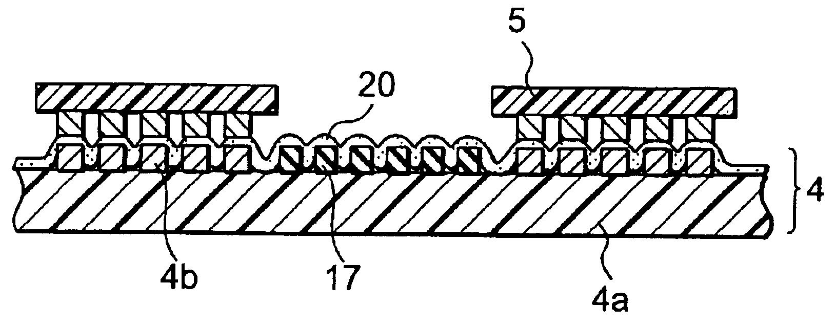
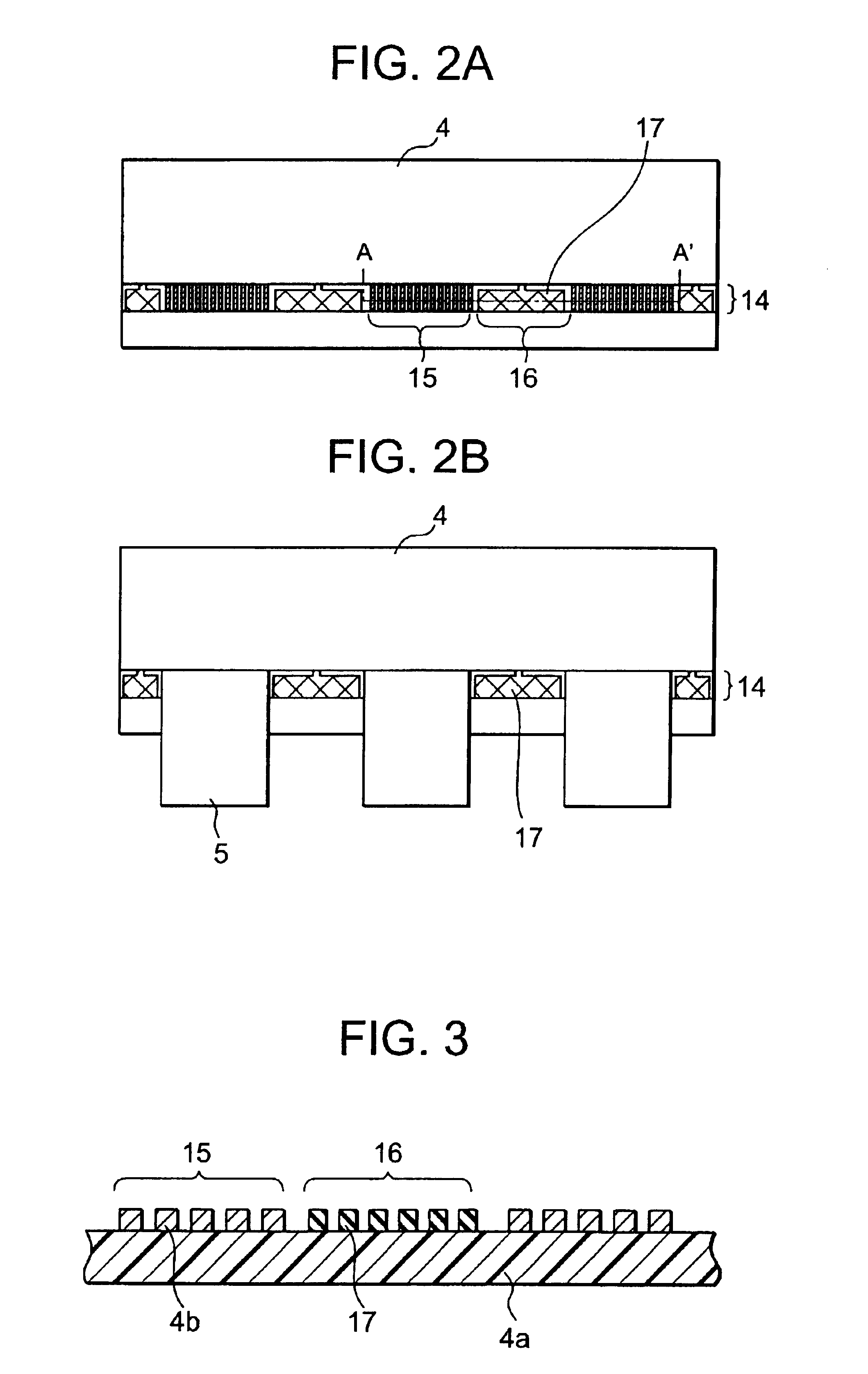
[0051]In a connecting structure according to a preferred embodiment of the present invention, for connecting flexible substrates connected to terminal portions of one of substrates constituting a liquid crystal display panel to connecting substrates through an electrically conductive adhesive film such as an anisotropic conductive film (ACF), bonding assist members each formed of the same material as that of an internal wiring or the connecting terminal of the connecting substrate and having substantially the same height as that of the connecting terminal is provided between adjacent terminal groups. The terminal groups each including a plurality of connecting terminals are provided in terminal forming regions of a non-coating portion of the connecting substrate, which is provided in the vicinity of a side portion thereof by removing a protective coating resin thereon, to relax a step between a terminal group in the terminal forming region in the non-coating portion and an exposed r...


PUM

PropertyMeasurementUnit
pressureaaaaaaaaaa
temperatureaaaaaaaaaa
pressureaaaaaaaaaa

Abstract

In connecting a connecting substrate 4 to a flexible substrate 5 connected to a terminal portion of one of substrates constituting a liquid crystal display panel through an anisotropic conductive film (ACF) 20, a bonding assist member 17 formed of the same material as that of an internal wiring or a connecting terminal of the connecting substrate and having substantially the same height as that of the connecting terminal is provided between adjacent terminal groups each including a plurality of connecting terminals 4b in a terminal forming region of a non-coating portion 14 in the vicinity of the connecting substrate 4, to absorb a difference in height between the terminal groups and the non-coating portion by the bonding assist member 17 to thereby make the ACF in an intimate contact with the terminal groups as well as the exposed regions uniformly throughout thereof during a temporary press-bonding step of the ACF and prevent a peeling-off and/or breakage of the ACF between the terminal groups and improve the reliability of electrical connection.

Description

BACKGROUND OF THE INVENTION[0001]1. Field of the Invention[0002]The present invention relates to a connecting structure of a circuit substrate and, in particular, the present invention relates to a connecting structure for connecting flexible substrates and a circuit board of a liquid crystal display device and to a liquid crystal display having the same connecting structure. The present invention further relates to a mounting method of the liquid crystal display device.[0003]2. Description of the Prior Art[0004]A liquid crystal display has been widely used in a field of OA (Office Automation) devices, AV (Audio-video) devices and portable terminals, etc., due to its thin and lightweight structure and low power consumption characteristics thereof. The liquid crystal display device is generally constructed with a liquid crystal panel composed of a TFT substrate on which thin film transistors are provided as switching elements, an opposing substrate and liquid crystal sealed in a gap ...

Claims


Application Information

Patent Timeline
Patent Type & Authority Patents(United States)
IPC IPC(8): H05K3/36G02F1/13H05K3/32H05K1/11H05K1/14G02F1/1345G09F9/00G09F9/30G09F9/35H05K1/02
CPCH05K3/361G02F1/13452H05K1/117H05K1/142H05K2201/09781H05K2201/09681H05K3/323G02F1/1345
Inventor SATONAKA, MASAHARU
Owner HANNSTAR DISPLAY CORPORATION
Why Eureka
Try Eureka