System and method for reducing trapped charge effects in a CMOS photodetector

a photodetector and complementary metal oxide semiconductor technology, applied in the field of light capture devices, can solve the problems of substantially incapable charge traps of storing the illumination-dependent charge that is later generated, substantially incapable charge traps of storing the illumination-dependent charge, etc., and achieve the effect of reducing the effect of electric charge trapped and reducing the effect of illumination-dependent trapped charge effects

Active Publication Date: 2005-07-05
APTINA IMAGING CORP
View PDF1 Cites 7 Cited by
  • Summary
  • Abstract
  • Description
  • Claims
  • Application Information

AI Technical Summary

Benefits of technology

[0010]The invention provides several embodiments of a system and method for reducing the effects of electric charge trapped in a CMOS photodetector. In one embodiment, the invention is a system for reducing illumination-dependent trapped charge effects in a complementary metal oxide semiconductor (CMOS) photodetector. The system comprises a negative-polarity voltage source connected to the photodetector via a first switch operable duri...

Problems solved by technology

The forward biasing charges all the charge traps in the photodetector, rendering the charge traps substantially incapable of storing the illumination-dependent charge that is later generated by the photodetector in response to incident illumination....

Method used


Image

  • System and method for reducing trapped charge effects in a CMOS photodetector
  • System and method for reducing trapped charge effects in a CMOS photodetector
  • System and method for reducing trapped charge effects in a CMOS photodetector

Examples


Embodiment Construction

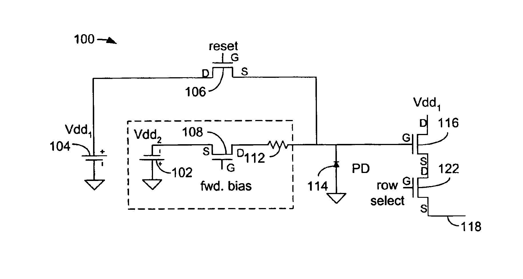
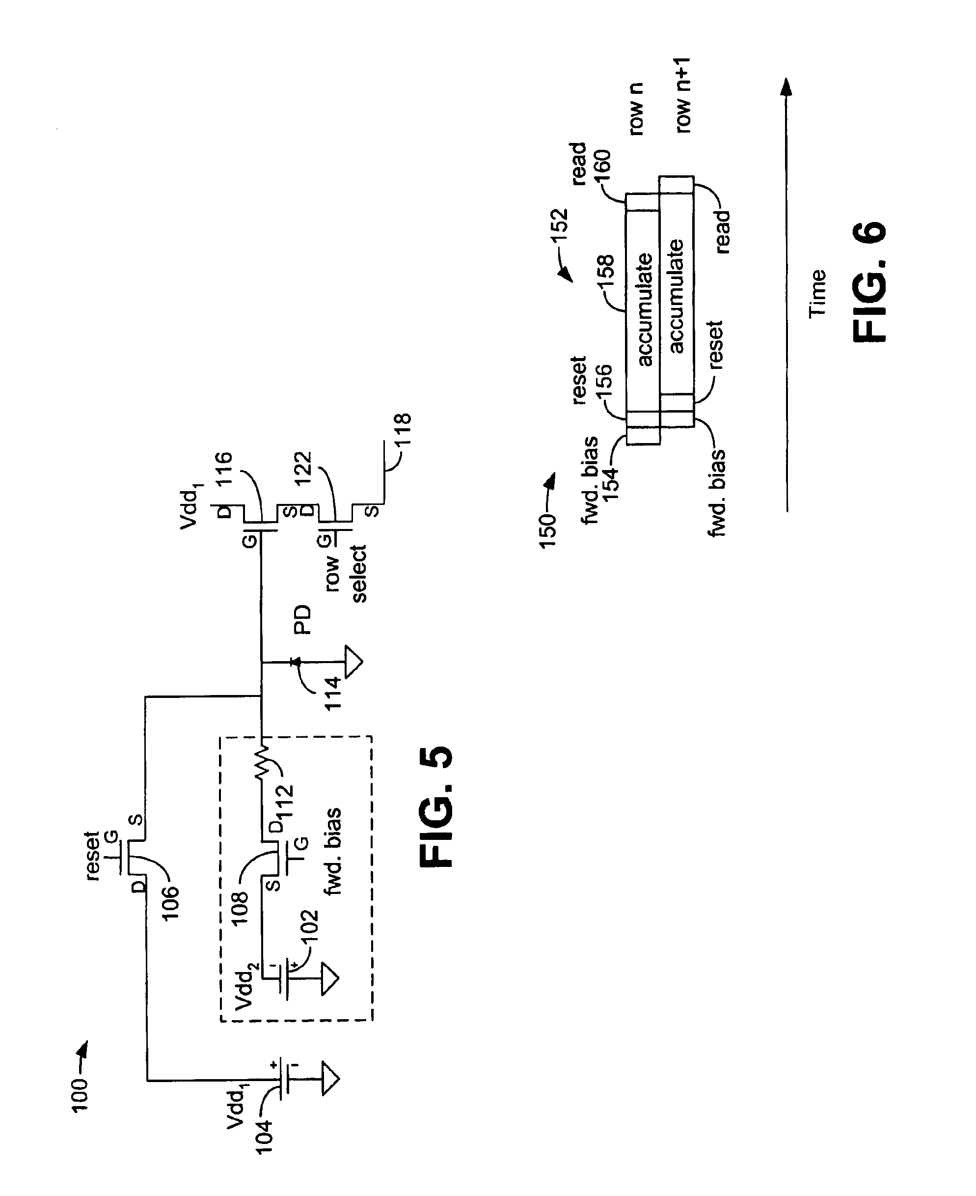
[0025]FIG. 5 is a schematic diagram illustrating a first embodiment of a pixel 100 constructed in accordance with the invention. The pixel 100 includes a photodetector 114, a pair of transistor switches 106 and 108, a resistor 112, a transistor 116, a transistor 122, a negative-polarity voltage source 102 and a positive-polarity voltage source 104. Although not shown in FIG. 5, the photodetector 114 is fabricated in a semiconductor layer comprising hydrogenated amorphous silicon, while the transistor switches 106 and 108, the resistor 112 and the transistors 116 and 122 are fabricated in a semiconductor layer comprising crystalline silicon.

[0026]The anode of the photodetector 114 is connected to ground. The negative-polarity voltage source 102 is coupled to the cathode of the photodetector 114 via the transistor switch 108 and a resistor 112. Specifically, the source of the transistor switch 108 is connected to the negative-polarity voltage source 102 and the drain is connected to t...


PUM


Abstract

A system and method for reducing image lag in a complementary metal oxide semiconductor (CMOS) photodetector is disclosed. In one embodiment, the invention is a a method for reducing image lag in an array of complementary metal oxide semiconductor (CMOS) photodetectors by forward biasing the photodetectors during a first time period to charge charge traps in the photodetectors, and reverse biasing the photodetectors during a second time period to remove charge from the photodetectors except the charge trapped in the charge traps.

Description

TECHNICAL FIELD[0001]The invention relates generally to light-capturing devices, and, more particularly, to a system and method for reducing trapped charge effects in a complementary metal oxide semiconductor (CMOS) photodetector.BACKGROUND OF THE INVENTION[0002]Electronic image sensors are widely used in a variety of electronic cameras and scanners. Historically, most of these sensors have been implemented as charge-coupled devices (CCD). A CCD converts photons captured in individual picture elements (pixels) into electrical charge. In a CCD, complicated clock voltages and high voltage potentials are required to transfer the electric charge that results from the absorption of photons out of the pixel. More recently CMOS active pixel sensors (APS) have been developed. A CMOS active pixel sensor is preferred over a CCD because the circuit that generates the requisite timing signals can be integrated on the same chip with the pixel circuit and because a CMOS active pixel sensor operat...

Claims


Application Information

Patent Timeline
IPC IPC(8): H01L21/00H01L31/00H01L27/00H01L27/146H04N5/357H04N5/374
CPCH04N5/3597H04N5/37452H01L27/14643H04N25/626H04N25/771
Inventor BAER, RICHARD L.
Owner APTINA IMAGING CORP
Why Eureka
Try Eureka