Flat panel display with nanotubes

a technology of nanotubes and flat panels, which is applied in the manufacture of electric discharge tubes/lamps, tubes with screens, discharge tubes luminescent screens, etc., can solve the problems of difficult to obtain uniform electron emission characteristics in a plane, low emission point density, and further deformation of electron emission points, so as to increase the electron emission point density and uniform electron emission characteristics , the effect of uniform electron emission characteristics

Inactive Publication Date: 2005-07-05
PANASONIC LIQUID CRYSTAL DISPLAY CO LTD +1
View PDF8 Cites 31 Cited by
  • Summary
  • Abstract
  • Description
  • Claims
  • Application Information

AI Technical Summary

Benefits of technology

[0003]In this method, however, the ratio of part of carbon nanotubes which is oriented in a direction vertical to the substrate and on which an electric field is liable to be concentrated is small, with the result that the electron emission point density is low, amounting to 100 electrons / cm2 or less, to make it difficult to obtain uniform electron emission characteristics in a plane. Further, resin and glass intrude into a portion where a metal fine particle contacts a fine fibered substance and as a result, the contact resistance between the metal fine particle and the fine fibered substance becomes large and the ratio of part of fine fibered substances which makes contact to the metal fine particles is reduced drastically, raising a problem that the electron emission point is further degraded.
[0004]According to the present invention, fine recess structures are formed on a metal film prepared on an electron emitter substrate and the fine fibered substances or carbon nanotubes are arranged on the fine recess structures, thereby ensuring that most of the fine fibered substances or carbon nanotubes can be oriented vertically to the substrate. With this construction, the electric field can be concentrated on most of the fine fibered substances or carbon nanotubes to drastically increase the electron emission point density and uniform electron emission characteristics can be realized in a plane.

Problems solved by technology

In this method, however, the ratio of part of carbon nanotubes which is oriented in a direction vertical to the substrate and on which an electric field is liable to be concentrated is small, with the result that the electron emission point density is low, amounting to 100 electrons / cm2 or less, to make it difficult to obtain uniform electron emission characteristics in a plane.
Further, resin and glass intrude into a portion where a metal fine particle contacts a fine fibered substance and as a result, the contact resistance between the metal fine particle and the fine fibered substance becomes large and the ratio of part of fine fibered substances which makes contact to the metal fine particles is reduced drastically, raising a problem that the electron emission point is further degraded.

Method used


Image

  • Flat panel display with nanotubes
  • Flat panel display with nanotubes
  • Flat panel display with nanotubes

Examples


first embodiment

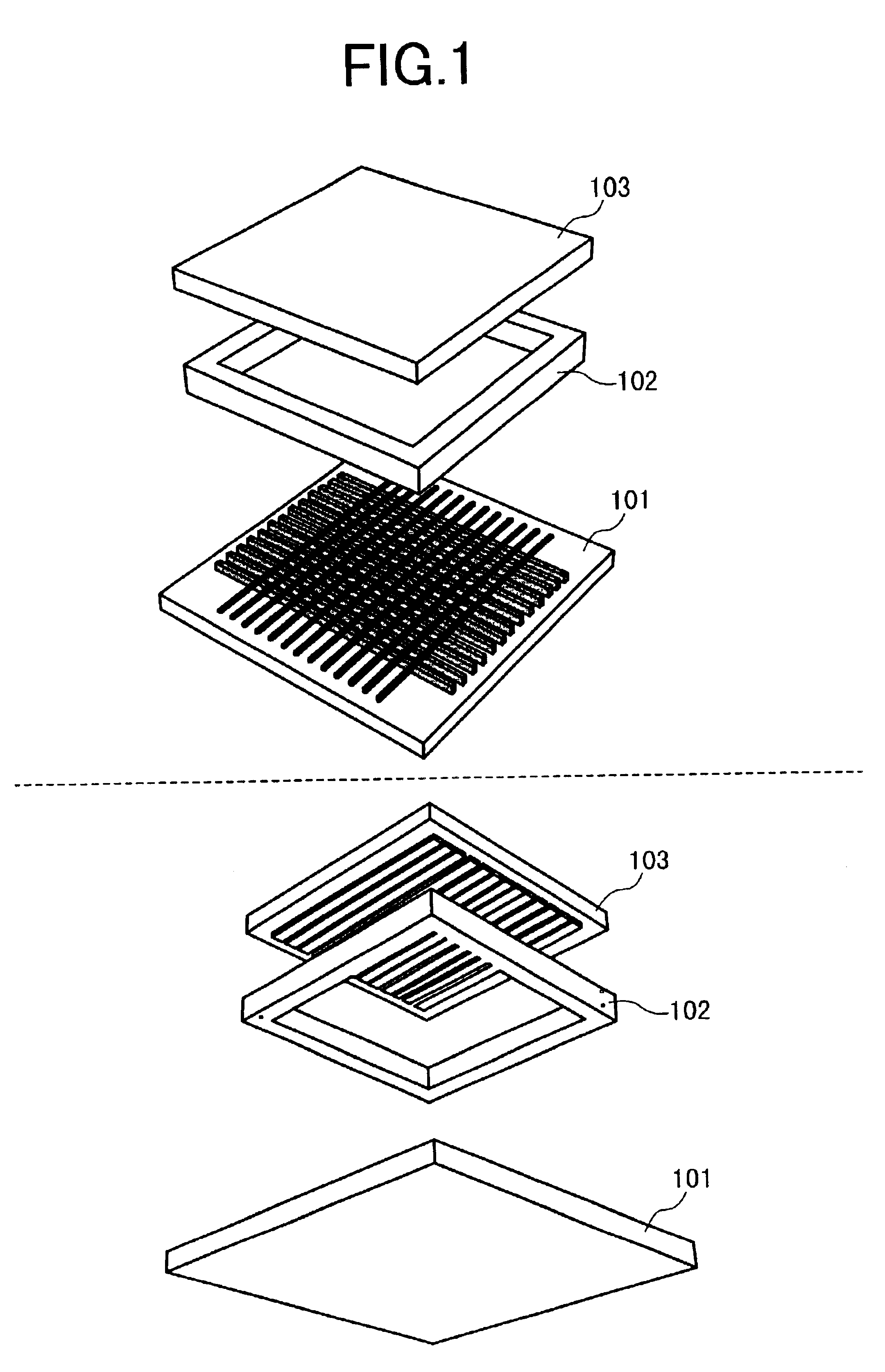
[0024]Referring to FIGS. 1, 2, 3, 4A to 4C, 5A to 5I and 6A to 6H as well as FIGS. 17 and 18, the present invention will now be described. Firstly, the overall construction of a flat panel display of spontaneous luminescent type according to the invention will be described with reference to FIG. 1. The present display comprises an electron emitter plate 101 provided with electron emitter arrays, a phosphor plate 103 provided with phosphor stripes or dots in register with electron emitters, and a glass frame 102 for fixing the electron emitter plate 101 and phosphor plate 103 by spacing them at a constant distance. Although not illustrated, a spacer for keeping the electron emitter plate 101 and phosphor plate 103 spaced needs to be provided inside the glass frame as the screen size increases.

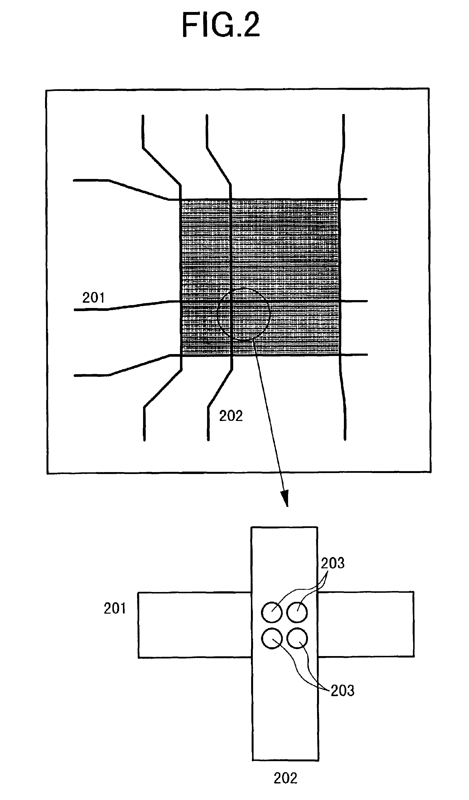
[0025]Next, the structure of the electron emitter plate will be described with reference to FIG. 2. A plurality of cathode electrode stripes 201 are formed in the horizontal direction and a plur...

third embodiment

[0048]Next, the invention will be described with reference to FIG. 8A as a plane view and FIG. 8B as a sectional view indicated by VIIIB—VIIIB on FIG. 8A, and FIG. 8C as a plane view and FIG. 8D as a sectional view indicated by VIIID—VIIID on FIG. 8C.

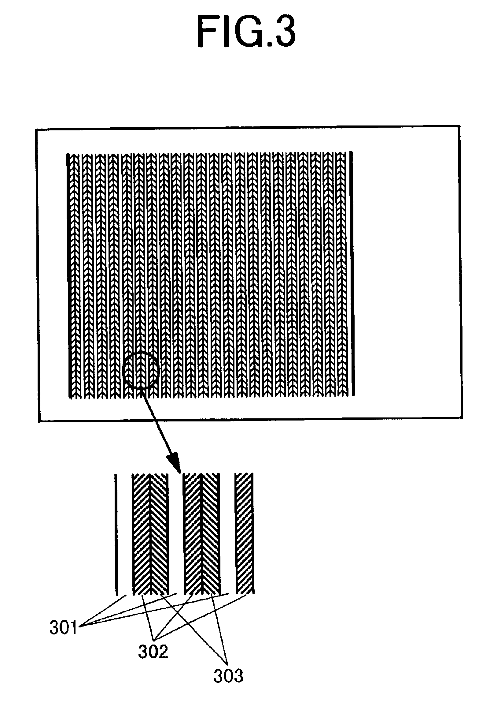
[0049]The third embodiment differs from the first embodiment in the method for formation of fine recess structures on the surface of the cathode electrode. Firstly, 600 cathode electrode stripes each having a width of 300 μm are formed at intervals of 60 μm by screen-printing Ni paste containing Ni fine particles of 1 μm average diameter on a glass substrate. A resulting structure is sintered at 550° for 30 minutes in the atmosphere, thus having a film thickness of 10 μm.

[0050]FIG. 8A shows a plane view and FIG. 8B shows a sectional view indicated by VIIIB—VIIIB on FIG. 8A of the cathode electrode stripe 801. Subsequently, gold is vapor-deposited on the entire surface to a thickness of 0.1 μm and thereafter, the ordinary photolithograph...

fourth embodiment

[0055]Next, the invention will be described with reference to FIGS. 9A to 9C and FIGS. 10A to 10I. Referring first to FIGS. 9A to 9C, the structure of the electron emitter plate will be described. FIG. 9A is a plane view, FIG. 9B is a sectional view indicated by IXB—IXB on FIG. 9A and FIG. 9C is a sectional view indicated by IXC—IXC on FIG. 9A.

[0056]Firstly, 600 cathode electrode stripes 901 each having a thickness of 0.2 to 10 μm and a width of 300 μm are formed at intervals of 60 μm on the surface of a glass substrate. Subsequently, an insulating layer 905 is formed. The insulating layer 905 has a thickness of 1 to 50 μm and structurally, it is formed with electron emitter holes 903 each having a diameter of 1 to 50 μm at each intersection of the cathode electrode stripe 901 and gate electrode stripe 902. After the insulating layer 905 is sintered at 550° C., 2400 gate electrode stripes 902 each having a thickness of 0.2 to 10 μm and a width of 90 μm are formed at intervals of 30 ...


PUM

PropertyMeasurementUnit
depthaaaaaaaaaa
lengthaaaaaaaaaa
thicknessaaaaaaaaaa

Abstract

A flat panel display includes an electron emitter plate provided with electron emitters, a phosphor plate provided with phosphors and a space defined by the electron emitter plate and the phosphor plate for form a substantial vacuum atmosphere therebetween, wherein a great number of fine recess structures are formed on the surface of a metal film formed on the electron emitter plate, and fine fibered substances or carbon nanotubes or substances containing the fine fibered substances or carbon nanotubes are arranged on the fine recess structures to form electron emitters.

Description

BACKGROUND OF THE INVENTION[0001]The present invention relates to a spontaneously luminescent type flat panel display using, as electron emitters, substances having a fine fibered structure such as carbon nanotubes.[0002]Conventionally, when substances having fine fibered structures such as carbon nanotubes are used as electron emitters, a method has been used generally in which the fine fibered substances are mixed with, for example, metal fine particles, resin and glass and a resulting mixture is printed on a substrate. An example of fabricating a 4.5-inch spontaneous luminescent type flat panel display by using this method is described in SID 99 Digest, pp. 1134-1137.SUMMARY OF THE INVENTION[0003]In this method, however, the ratio of part of carbon nanotubes which is oriented in a direction vertical to the substrate and on which an electric field is liable to be concentrated is small, with the result that the electron emission point density is low, amounting to 100 electrons / cm2 ...

Claims


Application Information

Patent Timeline
Patent Type & Authority Patents(United States)
IPC IPC(8): H01J1/304H01J1/30H01J9/02H01J31/12
CPCB82Y10/00H01J1/3048H01J9/025H01J2329/00Y10S977/952C01B32/05H01J1/30
Inventor OKAI, MAKOTOMUNEYOSHI, TAKAHIKOYAGUCHI, TOMIOHAYASHI, NOBUAKI
Owner PANASONIC LIQUID CRYSTAL DISPLAY CO LTD
Why Eureka
Try Eureka