Active matrix display device

Inactive Publication Date: 2005-07-05
SEMICON ENERGY LAB CO LTD
View PDF65 Cites 86 Cited by
  • Summary
  • Abstract
  • Description
  • Claims
  • Application Information

AI Technical Summary

Benefits of technology

[0025]In FIG. 1D, it is possible to construct TFTs 131 to 136 by forming six intersections with the semiconductor region 100. This circuit is shown in FIG. 2D, and the TFT 122 in FIG. 2C is simply replaced with two serial TFTs. In

Problems solved by technology

However, since there are a large number of traps present within the semiconductor film, this PN junction is imperfect and a junction leak current is liable to flow.
The fact that the OFF current increases as the gate electrode is negatively biased is because the carrier density in the P-type layer formed in the surface of the semiconductor film increases and the width of the energy barrier at the PN junction becomes na

Method used


Image

  • Active matrix display device
  • Active matrix display device
  • Active matrix display device

Examples


embodiment 1

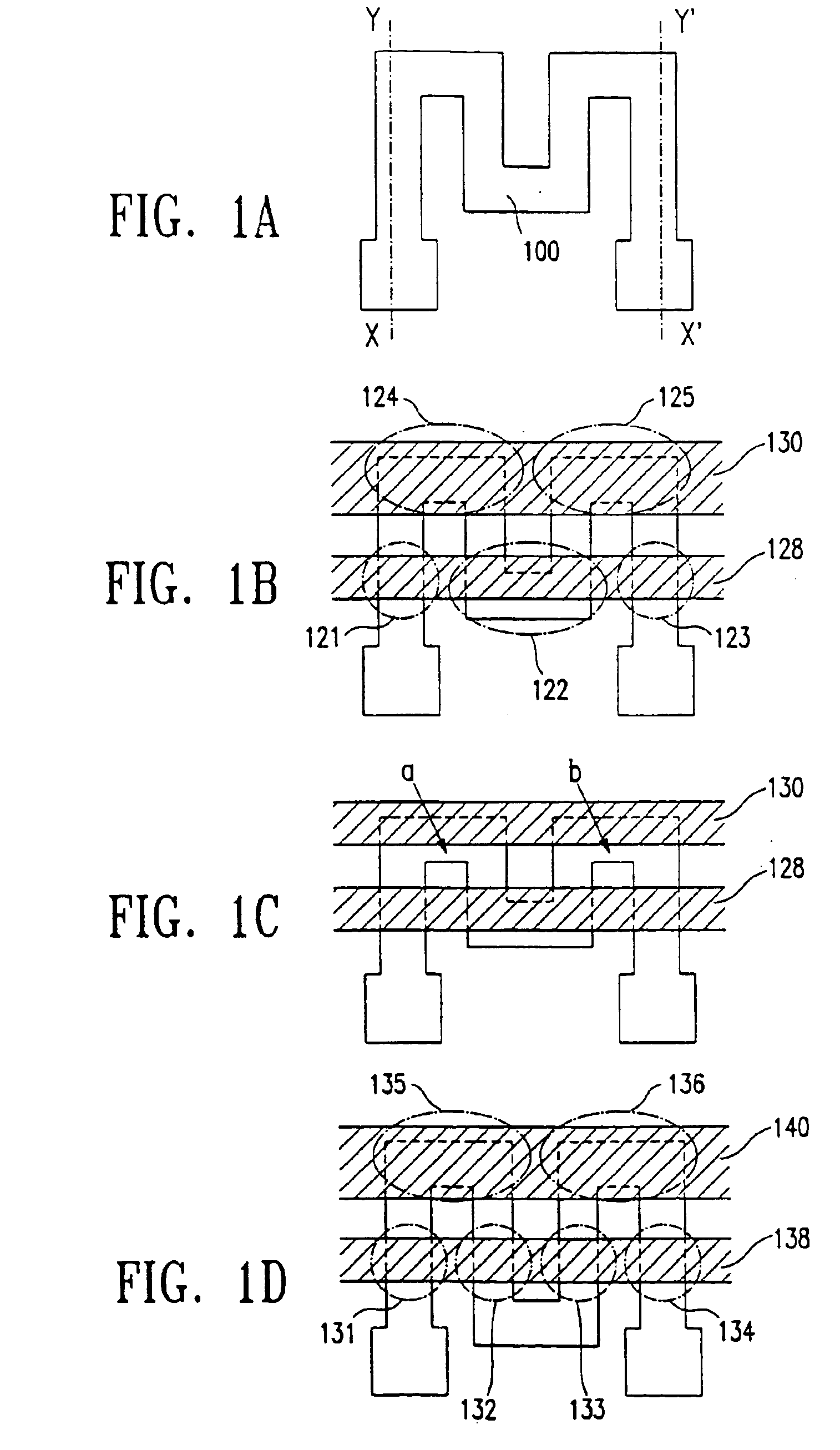
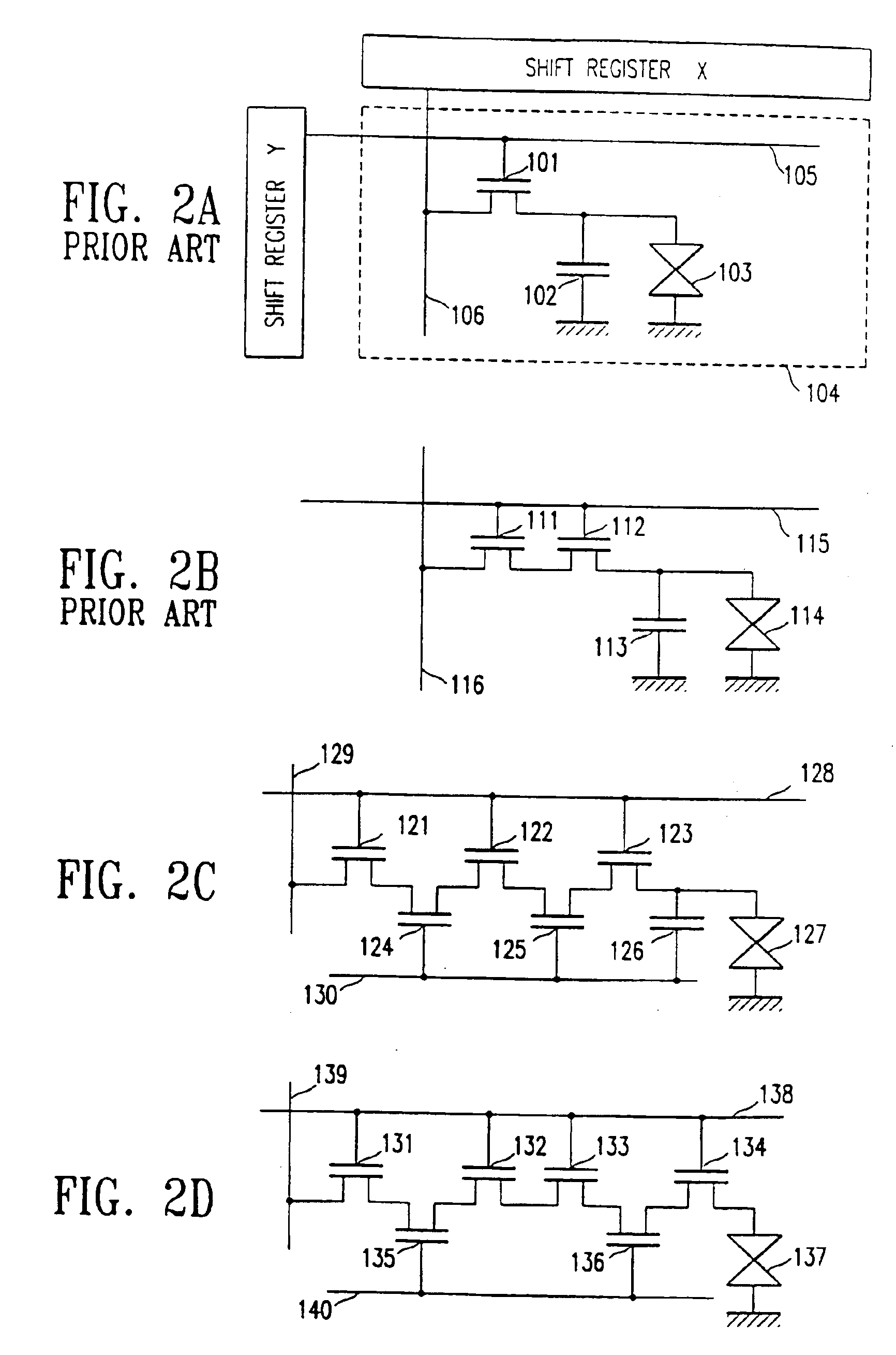
[0039]In the embodiment, an offset gate region and an LDD (lightly doped drain) region are constructed by anodizing a gate electrode to decrease an OFF current. A method for anodizing the gate electrode is disclosed in Japanese Patent Application Open No. 5-267667. FIGS. 1A to 1D show the circuit of the embodiment when viewed from above, and FIGS. 3A to 3F are a cross sectional view of the producing process. In the figures, the left side shows a cross section of the portion indicated by the dot-dash line X-Y in FIG. 1A, and the right side shows a cross section of the portion indicated by X′-Y′. They are drawn adjacent, but it should be noted that clearly X-Y and X′-Y′ are not on the same straight line.

[0040]A silicon oxide film 302 with a thickness of 1000 to 5000 Å, e.g., 3000 Å, is formed as a base film on a substrate (Corning 7059 glass, 100 mm×100 mm) 301. TEOS (tetraethoxysilane) is decomposed and deposited by plasma CVD (chemical vapor deposition) to form the silicon oxide fil...

embodiment 2

[0056]The embodiment is a modifying example of an LDD structure. FIGS. 1A to 1D show the circuit of the embodiment when viewed from above, and FIGS. 4A to 4F are a cross section view of the producing process. In the figures, the left side shows a cross section of the portion indicated by the dot-dash line X-Y in FIG. 1A, and the right side shows a cross section of the portion indicated by X′-Y′, as similar to FIGS. 3A to 3F. They are drawn adjacent, but it should be noted that clearly X-Y and X′-Y′ are not on the same straight line.

[0057]A silicon oxide film 402 having a thickness of 1000 to 5000 Å, e.g., 3000 Å, is formed as a base film on a substrate (Corning 7059 glass, 100 mm×100 mm) 401. TEOS is decomposed and deposited by plasma CVD to form the silicon oxide film 302. This process may also be performed by sputtering.

[0058]An amorphous silicon film having a thickness of 300 to 1500 Å, e.g., 500 Å, is deposited by plasma CVD or LPCVD and then left for 8 to 24 hours in an atmosph...

embodiment 3

[0070]FIGS. 5A to 5F show the process for forming the circuit in the embodiment. A detailed description of the specific processes is not given since a known method (or the method in embodiment 1) should be used.

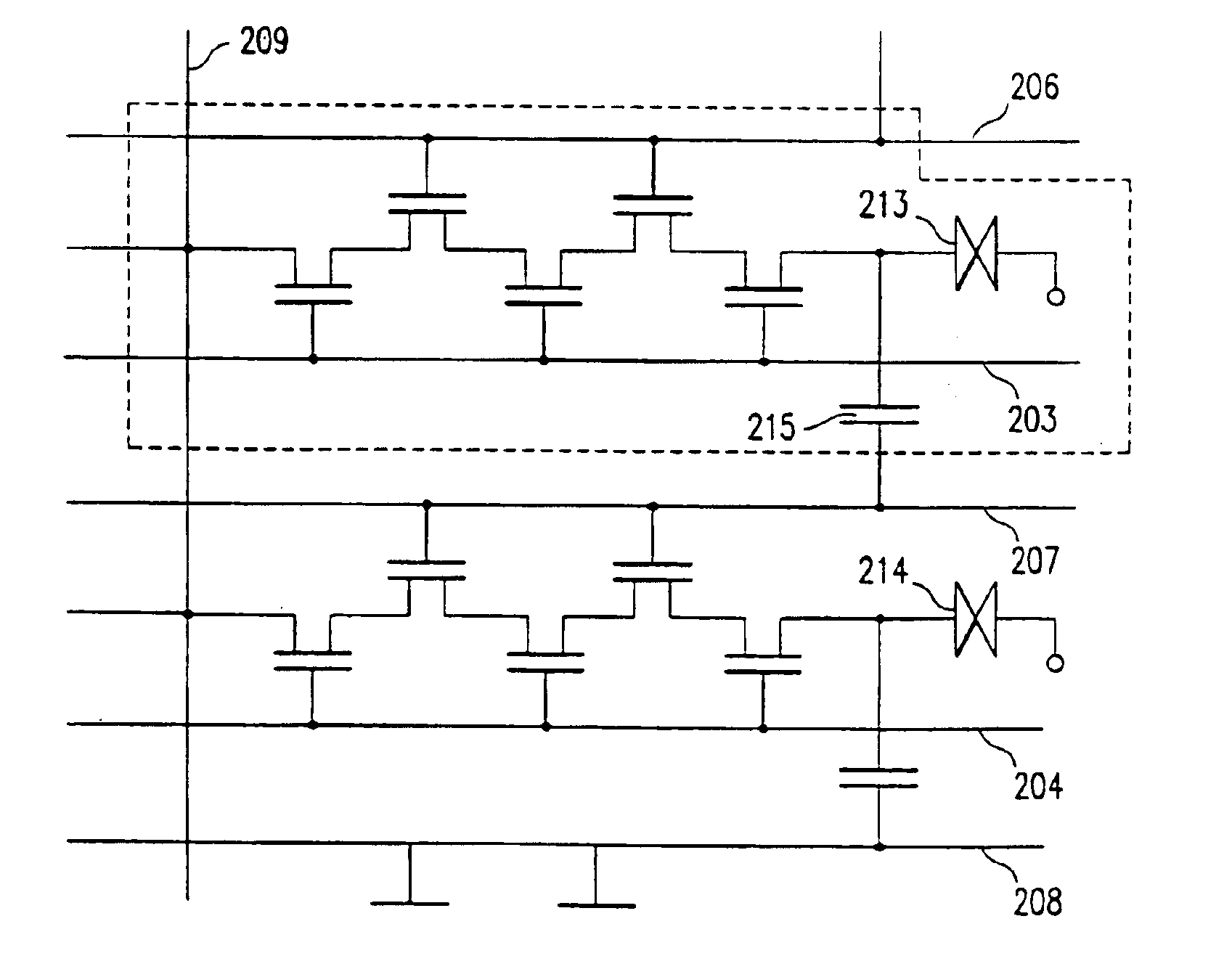
[0071]An approximately M-shaped semiconductor regions (active layers) 201 and 202 as in Embodiment 1 (or FIG. 1A) are formed. After a gate insulating film (not shown) is formed the gate signal lines 203 to 205 and the capacitance lines 106 to 208 are formed. The positional relationship between the gate signal lines, the capacitance lines and the active layers are the same as in Embodiment 1. (FIG. 5A)

[0072]After doping the active layers 201 to 204, an interlayer insulator is formed, and then the contact holes 210 and 211 are formed at the left ends of the active layers, thereby forming the image signal line 209. (FIG. 5B)

[0073]Pixel electrodes 212 to 214 are formed in regions surrounded by the gate signal lines and the image signal line. By the above processes, switching elem...


PUM


Abstract

In an active matrix display device, a circuit including at least five thin film transistors (TFTs) which are provided with an approximately M-shaped semiconductor region for a single pixel electrode and gate lines and a capacitances line which cross the M-shaped semiconductor region, is used as a switching element. Each of the TFT have offset regions and lightly doped drain (LDD) regions. Then, by supplying a selection signal to the gate lines, the TFTs are operated, thereby writing data to the pixel, while a suitable voltage is supplied to the capacitance line, a channel is formed thereunder and it becomes a capacitor. Thus the amount of discharge from the pixel electrode is reduced by the capacitor.

Description

CROSS-REFERENCE TO RELATED APPLICATIONS[0001]This application is a continuation of U.S. application Ser. No. 08 / 978,210, filed Nov. 25, 1997 now U.S. Pat. No. 6,417,896, which is a divisional of U.S. application Ser. No. 08 / 602,017 filed Feb. 15, 1996 now U.S. Pat. No. 5,729,308.BACKGROUND OF THE INVENTION[0002]1. Field of the Invention[0003]The present invention relates to circuits and elements for improving the image quality of the display screen of an active matrix type display device used in, for example, a liquid crystal display device, a plasma display device or an EL (electroluminescence) display device.[0004]2. Description of the Related Art[0005]FIG. 2A schematically shows a conventional active matrix display device. A region 104 shown by the broken line is a display region. Thin film transistors (TFTs) 101 are arranged at a matrix form in the region 104. The wiring connected to the source electrode of the TFT 101 is an image (data) signal line 106, and the wiring connected...

Claims


Application Information

Patent Timeline
IPC IPC(8): G02F1/13G02F1/1362G09G3/36G09G3/30H01L29/786H01L29/66G02F1/1368G02F1/136G02F1/133G09F9/30H01L21/336
CPCG02F1/13624G09G3/30G09G3/3648H01L29/78645H01L29/78696G02F1/136213G02F1/1368G09G2300/0809G02F1/133
Inventor YAMAZAKI, SUNPEIKOYAMA, JUNTAKEMURA, YASUHIKO
Owner SEMICON ENERGY LAB CO LTD
Why Eureka
Try Eureka