Low-power semiconductor memory device

a memory device and low-power technology, applied in semiconductor devices, digital storage, instruments, etc., can solve the problems of increased power consumption in standby state, inability to ignore leakage current in sram memory cells, power consumption, etc., to reduce power consumption, reduce leakage current, and reduce power consumption

Inactive Publication Date: 2005-07-05
RENESAS ELECTRONICS CORP
View PDF9 Cites 24 Cited by
  • Summary
  • Abstract
  • Description
  • Claims
  • Application Information

AI Technical Summary

Benefits of technology

[0011](1) In a LSI consolidating a logic circuit and an SRAM circuit, the power source of the logic circuit is cut off by the switch at the time of standby, and the SRAM circuit controls the substrate voltage of the MOS transistor so as to reduce the leakage current.
[0012](2) The power source of the control circuit for accessing the memory cell in the SRAM circuit is divided to be cut off, reducing the power consumption.
[0013](3) The SRAM circuit is divided so that some SRAMs hold data at the time of standby and other SRAMs not holding data cut off the power source to reduce the leakage current.

Problems solved by technology

The power consumption in the standby state of the system LSI is the leakage current of the MOS transistor in the circuit.
When the threshold voltage of the MOS transistor is lowered, the power consumption in the standby state is increased.
However, when the MOS transistor is made finer and a large-capacitance SRAM is mounted on the system LSI so as to lower the threshold voltage of the MOS transistor constructing the SRAM memory cell, the leakage current in the SRAM memory cell cannot be ignored.
The power source cannot be cut off so that the leakage current cannot be reduced.

Method used


Image

  • Low-power semiconductor memory device
  • Low-power semiconductor memory device
  • Low-power semiconductor memory device

Examples


Embodiment Construction

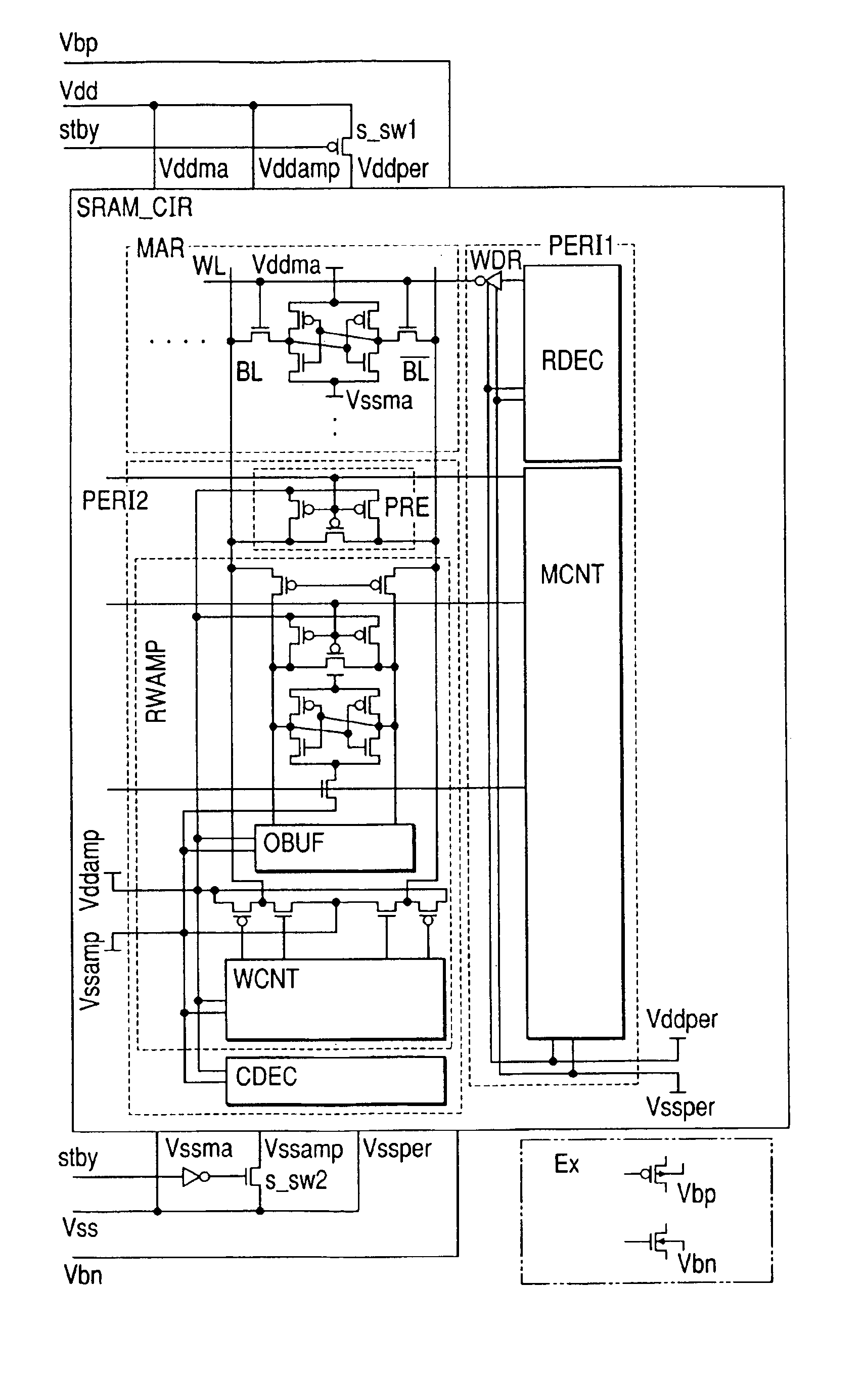
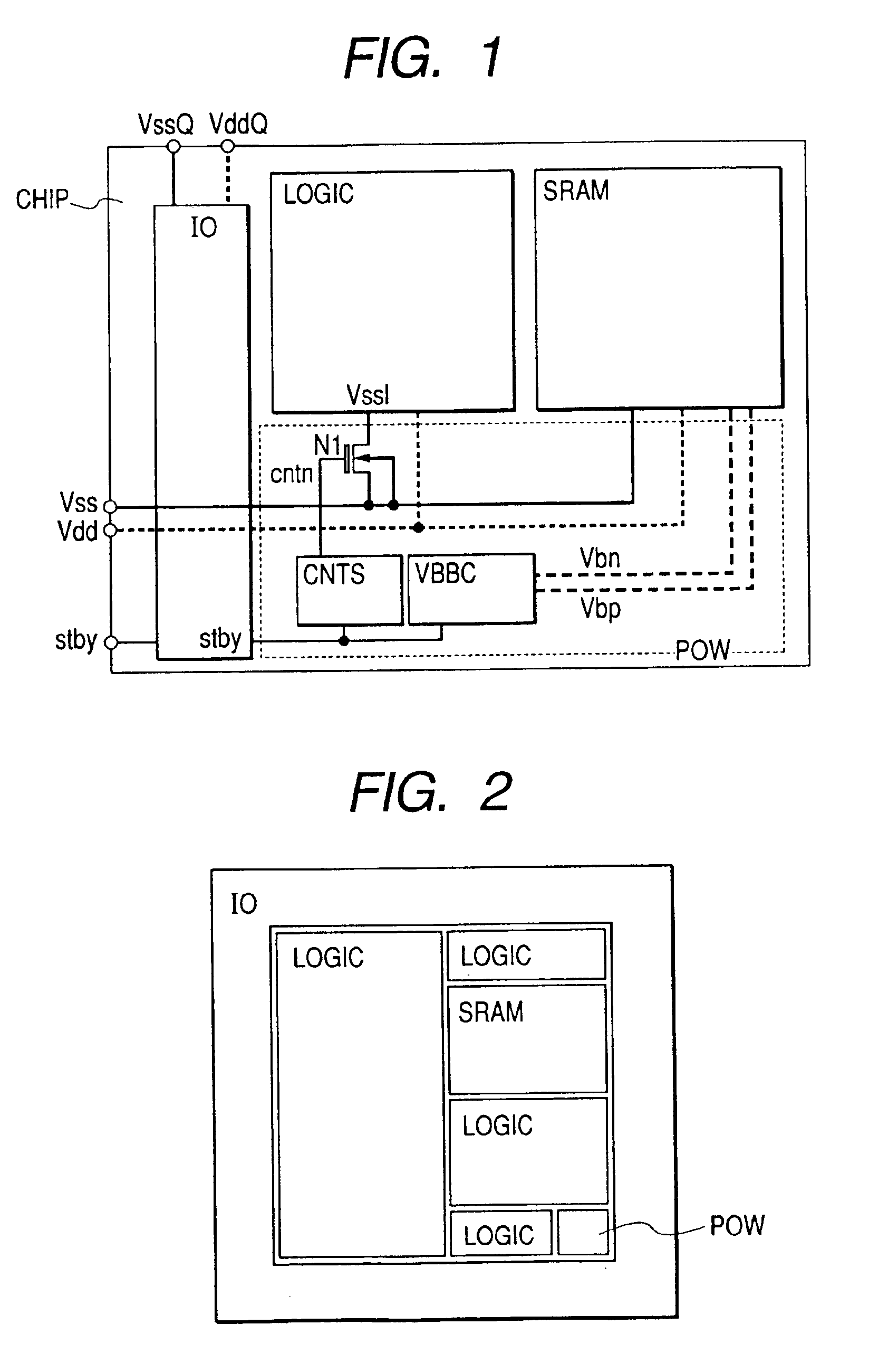
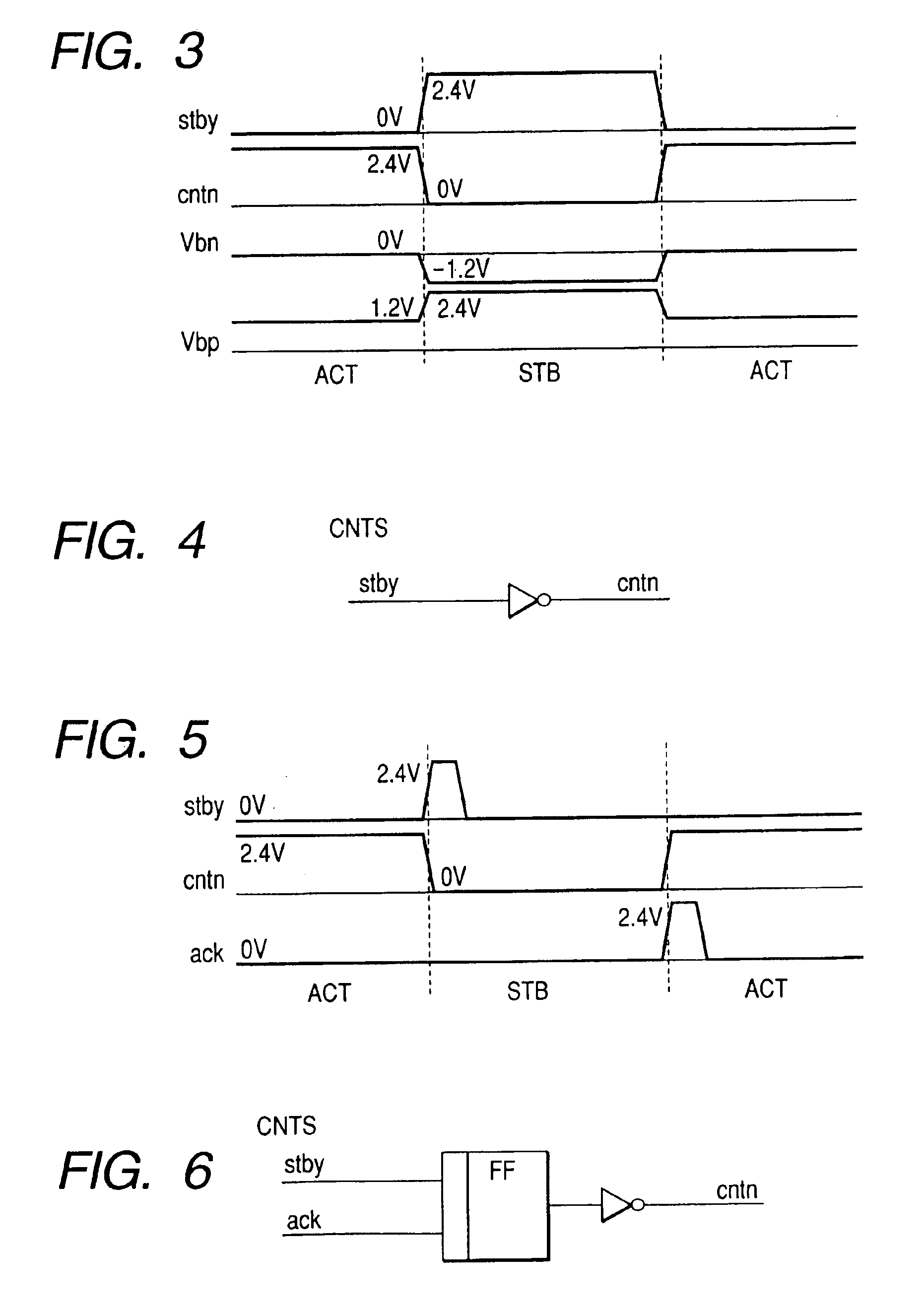
[0040]FIG. 1 schematically shows the entire construction of a LSI consolidating a logic circuit and an SRAM circuit using the present invention. In FIG. 1, a CHIP as the consolidated LSI includes an input / output circuit IO (IO circuit) having power voltage lines VssQ and VddQ from outside as operating voltages; a logic circuit LOGIC executing a predetermined process to data; a static memory circuit SRAM storing data; an nMOS transistor N1 as a switch between a ground voltage line Vss and an operating voltage supply line Vssl on the low voltage side of the logic circuit; a control circuit CNTS to which a signal stby inputted in the standby state is inputted to be connected to the gate electrode of the N1 outputting a signal cntn controlling the N1; and a substrate bias control circuit VBBC controlling substrate voltages Vbn and Vbp of the SRAM when the stby is inputted. Unless otherwise specified, the power source with a symbol starting from Vdd is a power source supplying a high vol...


PUM


Abstract

A logic circuit in a system LSI is provided with a power switch so as to cut off the switch at the time of standby, reducing leakage current. At the same time, an SRAM circuit of the system LSI controls a substrate bias to reduce leakage current.

Description

CROSS-REFERENCE TO RELATED APPLICATION[0001]This application is a division of application Ser. No. 10 / 274,985 filed Oct. 22, 2002 (now U.S. Pat. No. 6,657,911 issued Dec. 2, 2003).BACKGROUND OF THE INVENTION[0002]1. Field of the Invention[0003]The present invention relates to a semiconductor device consolidating a logic circuit and a static memory (SRAM) circuit.[0004]2. Description of the Related Art[0005]Japanese Published Unexamined Patent Application No. Hei 7-86916 discloses a construction in which a logic circuit is provided with a power switch and a MOS transistor constructing the logic circuit is back-gate biased. Japanese Published Unexamined Patent Application No. 2000-207884 discloses a substrate bias control technology for a system LSI operable at a low voltage including a static memory. Japanese Published Unexamined Patent Application No. 2001-93275 discloses a construction in which a logic circuit is provided with a logic power source and a memory circuit is provided w...

Claims


Application Information

Patent Timeline
Patent Type & Authority Patents(United States)
IPC IPC(8): G11C5/14G11C11/417G11C11/41G11C11/34G11C11/413G11C11/418H01L29/94
CPCG11C5/146G11C5/147G11C11/417G11C11/4125G11C2207/2227G11C7/1045G11C7/22G11C11/4074G11C11/4076G11C2207/104G11C11/34G11C11/419
Inventor YAMAOKA, MASANAOISHIBASHI, KOICHIROMATSUI, SHIGEZUMIOSADA, KENICHI
Owner RENESAS ELECTRONICS CORP
Why Eureka
Try Eureka