Circuit element with timing control

a technology of circuit elements and timing control, applied in the field of circuit elements with timing control, can solve the problems of inability to meet the needs of standby power, inability to adjust the timing of the circuit element,

Inactive Publication Date: 2005-07-05
POLARIS INNOVATIONS
View PDF7 Cites 18 Cited by
  • Summary
  • Abstract
  • Description
  • Claims
  • Application Information

AI Technical Summary

Benefits of technology

[0007]It is the object of the present invention to provide a device for the temporal control of at least one signal in a circuit element, which enables a compromise to be made between power consumption and accuracy.

Problems solved by technology

Each of these timers is subject to inaccuracies, chip area consumption and the need for standby power.
Alternative approaches have proved to be unsuitable.
Such approaches include e.g. the addition of a bit line supervisor to monitor the reset voltages, but the required chip area is too large.
On the other hand, the addition of a dummy bit line as reference leads to a high power consumption.
Furthermore, the generation of a delay which exactly fulfils a necessary specification is too difficult to implement.
Also, with this approach, all the timers must be specified externally, which is not possible since not all the memory elements which satisfy a standard necessarily have the same timer structure.

Method used


Image

  • Circuit element with timing control
  • Circuit element with timing control
  • Circuit element with timing control

Examples


Embodiment Construction

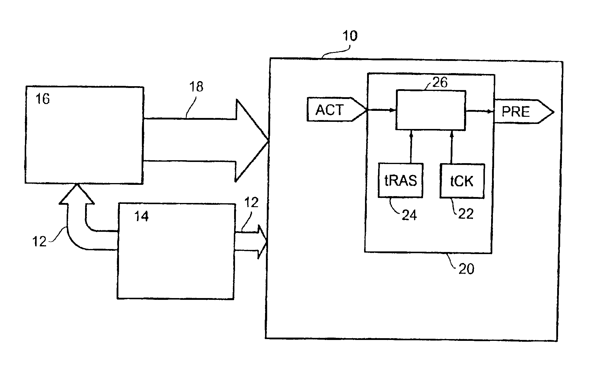
[0021]FIG. 1 shows a memory element 10, e.g. a DRAM element. The memory element 10 might also take the more specialized form of a DDR-SDRAM element (DDR SDRAM=double data rate synchronous dynamic random access memory).

[0022]The memory element 10 receives a clock signal 12 from a clock generator 14. The clock signal represents an external clock signal and possesses a certain clock frequency. Typical clock frequencies lie in a range between 83 MHz and 167 MHz. The clock generator 14 also supplies the clock signal 12 to an external control 16. The control 16 is connected to the memory element 10 via a signal bus 18, which is usually called the CMD bus. The memory element 10 can be a memory module with a plurality of memory chips on it or a single memory chip.

[0023]The control 16 communicates with the memory element 10 via the signal bus 18 so as to transfer control signals and data signals to the memory element 10 and to receive them from it.

[0024]So far the structure of the memory ele...


PUM


Abstract

A circuit element has an input for receiving an external clock with a clock period duration. A unit is provided to present the circuit element with information representing the clock period duration of the external clock. In addition the circuit element includes a unit for the temporal control of a signal in the circuit element on the basis of information representing the clock period duration.

Description

FIELD OF THE INVENTION[0001]The present invention relates to a circuit element with timing control and in particular to such a circuit element which receives an external clock with a clock frequency and an associated clock period duration. The present invention can be used to advantage particularly in the area of memory elements, e.g. DRAM elements (DRAM=dynamic random access memory).BACKGROUND OF THE INVENTION AND PRIOR ART[0002]Present day DRAM memory elements contain a plurality of chip-internal timers, i.e. on-chip timers, which control different processes running on the DRAM element. Each of these timers is subject to inaccuracies, chip area consumption and the need for standby power. Since present day DRAM memory elements are specified to operate in a wide frequency range, e.g. from 83 MHz to 167 MHz, the clock supplied to the memory element from the outside cannot be used as a time basis for the control of internal processes. In particular the external clock cannot be used to...

Claims


Application Information

Patent Timeline
Patent Type & Authority Patents(United States)
IPC IPC(8): G11C7/12G11C7/00G11C8/18G11C7/22G11C8/00G11C11/4094G11C11/409G11C11/4076G11C11/407
CPCG11C7/1066G11C7/12G11C7/22G11C7/222G11C8/18G11C11/4076G11C11/4094
Inventor KIEHL, OLIVER
Owner POLARIS INNOVATIONS
Why Eureka
Try Eureka