Delay adjustment circuit and a clock generating circuit using the same

a technology of delay adjustment and clock generating circuit, which is applied in the direction of generating/distributing signals, pulse techniques, instruments, etc., can solve the problem that the manufactured lsi may not operate, and achieve the effect of reducing jitter

Inactive Publication Date: 2005-07-12
NEC CORP
View PDF14 Cites 10 Cited by
  • Summary
  • Abstract
  • Description
  • Claims
  • Application Information

AI Technical Summary

Benefits of technology

[0010]In consideration of the above-described situation, a first object of the present invention is to provide a delay adjustment circuit that can adjust the delay time interval of an input signal by controlling internal register values and the internal signals of the semiconductor integrated circuit, or external signals. In addition, a second object of the present invention is to provide a clock generating circuit that can compensate the clock skew caused by manufacturing variations in the semiconductor integrated circuit device and the duty ratio, and in addition minimize jitter by using the delay adjustment circuit having a delay time interval that can be regulated by controlling the internal register values and the internal signals of the semiconductor integrated transistor device and external signals.
[0016]According to the clock generating circuit described in the fourth aspect, a delay adjustment circuit that can adjust the waveform without using a PLL circuit is used, and thereby the clock skew caused by production variation in the semiconductor integrated circuit device and the duty ratio can be compensated, and the jitter can be minimized.
[0018]According to the semiconductor integrated circuit device described in the fifth aspect, a flip flop that operates at the timing of a specified adjustable edge in the clock generating circuit is provided between logic gates, and thereby the influence of clock skew and jitter can be suppressed to a minimum.
[0024]According to the clock generating circuit described in the eighth aspect, the delay adjustment circuit described in either of the second or third aspects provides a clock skew detecting device that detects clock skew and a control device that automatically updates the register values in the delay adjustment circuit so that the clock skew becomes a pre-set expected value based on the detected output of the clock skew detecting device, and thereby the clock skew can be automatically adjusted so as to become a pre-set expected value.
[0026]According to the clock generating circuit described in the ninth aspect, a PPL circuit is not used, the clock waveform can be controlled, and thereby the jitter produced during operation of the semiconductor integrated circuit device (LSI) can be reduced, and the clock waveform can be adjusted with respect to the clock skew and fluctuations in the duty cycle of the clock caused by production variations in the transistor function, wiring width, and wiring thickness in the LSI.

Problems solved by technology

There is the problem that if the jitter is large and the duty function differs from estimates assumed during the design, the manufactured LSI may not operate, and then must be remanufactured or redesigned.

Method used


Image

  • Delay adjustment circuit and a clock generating circuit using the same
  • Delay adjustment circuit and a clock generating circuit using the same
  • Delay adjustment circuit and a clock generating circuit using the same

Examples


first embodiment

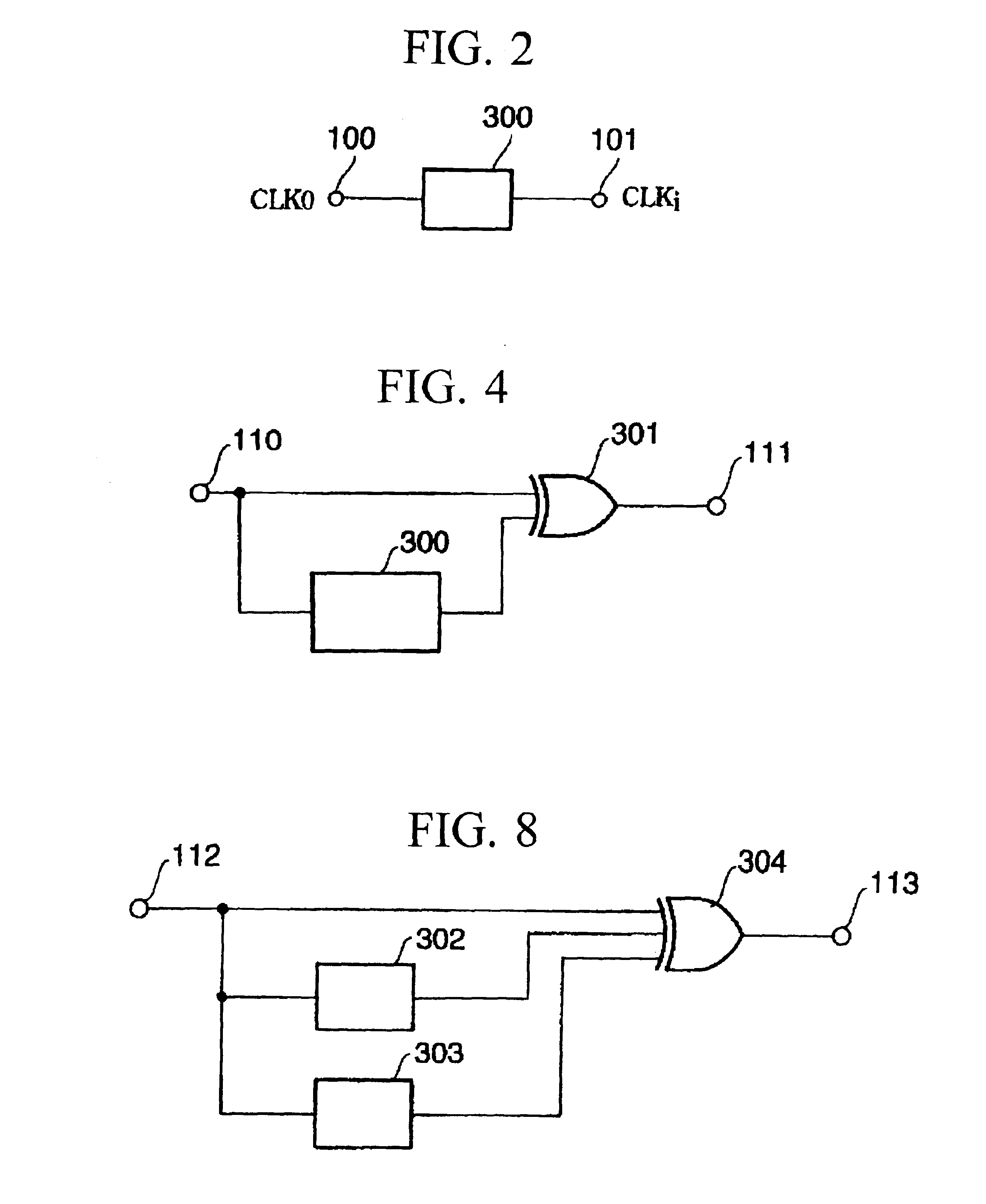
[0055]Next, the structure of the clock generating circuit according to the present invention is shown in FIG. 4.

[0056]The clock generating circuit according to the present embodiment comprises a delay adjustment circuit 300 having the structure described in FIG. 1, whose input signal is the reference clock CLK0, and the exclusive OR circuit 301 that carries out an exclusive OR operation on the reference clock CLK0 and the output signal of the delay adjustment circuit 300.

[0057]In the above-described structure, when a clock CLLj delayed by ¼ of a cycle by the delay adjustment circuit 300 with respect to a reference clock CLK input into the input terminal 110 is generated and the exclusive OR of the reference clock CLK0 and the clock CLLj is taken by the exclusive OR circuit 301, a clock CLKn having an operating frequency twice that of the reference clock CLK0 can be generated. Because the waveform of the clock CLLj can be adjusted by controlling the register values, the falling edge ...

second embodiment

[0061]Next, the structure of the present invention is shown in FIG. 7. The clock generating circuit according to this embodiment comprises the delay adjustment circuit shown in FIG. 1 that inputs the reference clock, an exclusive OR circuit 120 serving as a logic circuit that carries out logical processing of the reference clock and the output signal in the delay adjustment circuit and outputs the clock having an operational frequency N times the reference clock, and a PMOS transistor 110 serving as a setting device that fixes the output of the delay adjustment circuit to a constant value only during non-operational mode, and outputs a clock having an operational frequency equal to the reference clock when serving as a non-operational mode or N times (in the present embodiment, two times) the reference clock when serving as the operational mode based on the result of the logical processing of the exclusive OR circuit 120.

[0062]The delay adjustment circuit is essentially identical to...

third embodiment

[0064]The clock generating circuit according to the present invention is shown in FIG. 8 and the output timing of the relevant clock and each part of the output clock is shown in FIG. 9. In the clock generating circuit in FIG. 4, a clock that is delayed ¼ of a cycle by the delay adjustment circuit 300 is generated, but in the clock generating circuit shown in FIG. 8, a clock CLKx that is delayed ⅙ of a cycle by the delay adjustment circuit 302 and a clock CLKy that is delayed ⅓ of a cycle by the delay adjustment circuit 303 are generated.

[0065]When the exclusive OR of the reference clock CLK0, the clock CLKx delayed by ⅙ a of cycle, and the clock CLKy delayed by ⅓ of a cycle is taken by the exclusive OR circuit 304, a clock CLKz that has a controllable waveform and has an operating frequency three times the reference clock CLK0 can be generated. Similarly, according to the present embodiment, by using the reference clock as the input and carrying out logic processing of the output o...


PUM


Abstract

The present invention provides for adjusting the delay time interval of an input signal by controlling the internal register value and internal signal in a semiconductor integrated circuit device, or an external signal. The invention comprises a first gate array 10 for carrying out fine adjustment of the delay time interval of the input signal, capacitances 60 to 63 and 70 to 73 connected to the output side of a specified gate in the first gate array via first switching device 40 to 43, a second gate array 20 for carrying out rough adjustment of the delay time interval of the input signal; and a control device 30 that adjusts the delay time interval of the input signal by adjusting the capacitances connected to the output side of a specified gate in the first gate array and the number of gate stages in the second gate array 20.

Description

BACKGROUND OF THE INVENTION[0001]1. Field of the Invention[0002]The present invention relates to a delay adjustment circuit having an adjustable waveform that is used to generate a clock signal employed during digital processing and a clock generating circuit that generates a clock having a pre-determined frequency using this delay adjustment circuit.[0003]2. Description of the Related Art[0004]In a conventional clock generating circuit, in order to generate a clock that is 0.5×N (N=3, 4, 5, . . . ) times the operating frequency of a reference clock, a PLL circuit is frequently used. As shown in FIG. 14, a generally used PLL circuit 800 is formed by a phase comparing circuit 802, a low pass filter (LPF) 804, a voltage control oscillator (VCO) 806, and a 1 / N divider 808. Reference numeral 810 is a clock distributing circuit that supplies to each part the clock generated by the PPL circuit 800.[0005]This PLL 800 generates a clock 807 having an operating frequency that is N-times the r...

Claims


Application Information

Patent Timeline
Patent Type & Authority Patents(United States)
IPC IPC(8): H03K5/13H03L7/08H03L7/081H03K5/00G06F1/06G11C11/4076H03K5/04H03K5/131H03K5/135
CPCH03L7/0814H03L7/0818H03K5/133H03K2005/00071
Inventor YOSHIKAWA, ATSUSHIHAGIHARA, YASUHIKO
Owner NEC CORP
Why Eureka
Try Eureka