Optical information processing apparatus

a technology of optical information and processing apparatus, which is applied in the field of optical information processing apparatus, can solve the problems of increasing the error rate of signal reproduction circuit, difficult to maintain a low error rate in the reproduction of information,

Inactive Publication Date: 2001-01-09
PANASONIC CORP
View PDF4 Cites 3 Cited by
  • Summary
  • Abstract
  • Description
  • Claims
  • Application Information

AI Technical Summary

Problems solved by technology

Therefore, selecting a small minimum mark length for increased recording density results in an increased intersymbol interference (which is essentially the influence from preceding and subsequent marks), thereby making it difficult to maintain a low error rate in the reproduction of inf

Method used


Image

  • Optical information processing apparatus
  • Optical information processing apparatus
  • Optical information processing apparatus

Examples


example 2

(Example 2)

Hereinafter, a circuit for optimizing the delay time T of the aforementioned delay circuit 202 and the gain A of the aforementioned amplifier circuit 203 will be described with reference to FIG. 8.

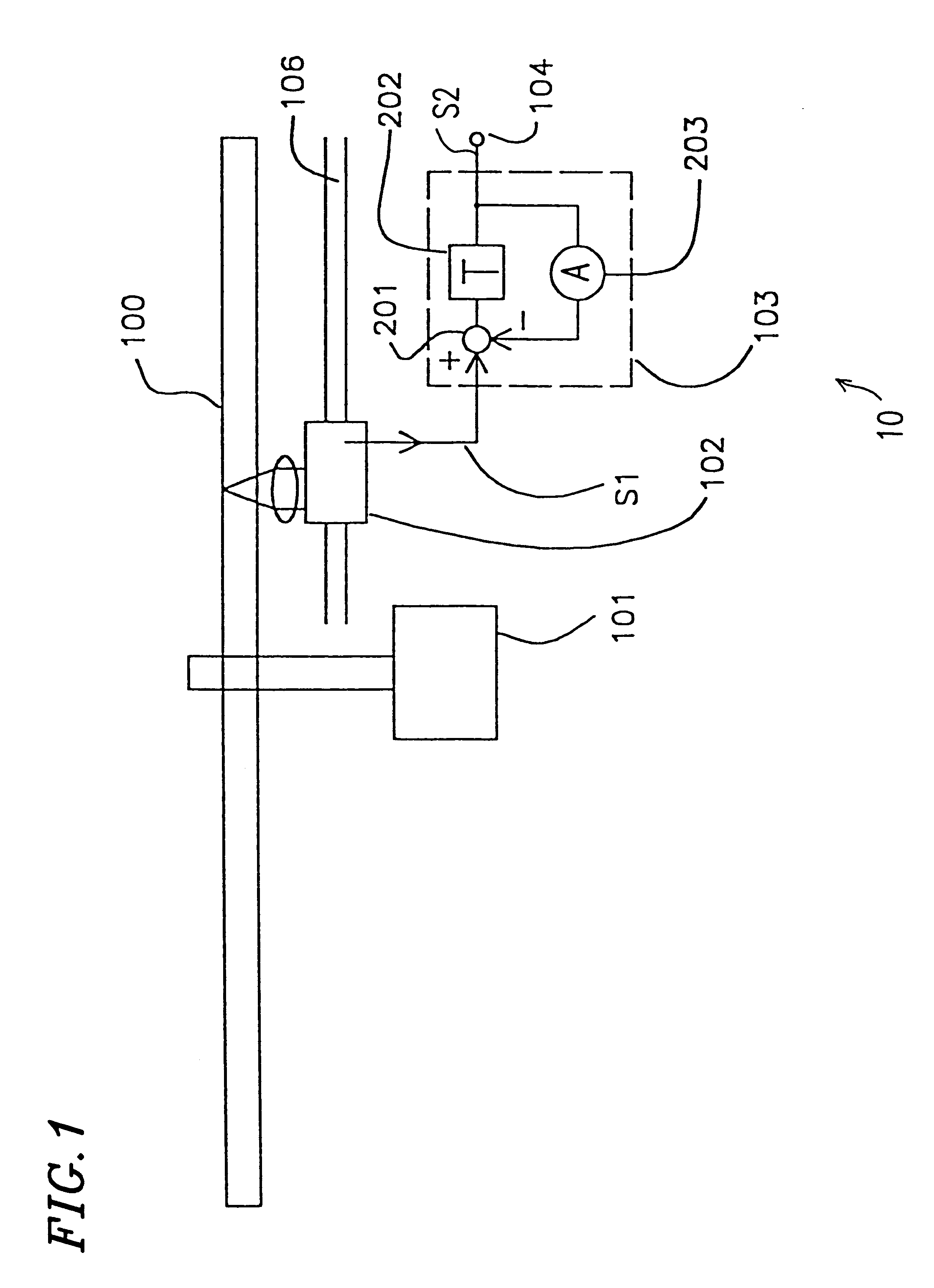
FIG. 8 is a block diagram illustrating an optical information processing apparatus 20 according to Example 2 of the present invention. The optical information processing apparatus 20 includes an optical head 102, a transportation member 106, a signal processing circuit 103, a jitter detection circuit 212, and a control circuit 213.

The control circuit 213 optimizes the signal processing circuit 103 so as to minimize the jitter value of the reproduction signal S2 output from the signal processing circuit 103. Specifically, the control circuit 213 optimizes the delay time T and the gain A so as to minimize the jitter value of the reproduction signal S2.

The jitter detection circuit 212 receives the reproduction signal S2 which is output from a terminal 104 of the signal processing c...

example 3

(Example 3)

Hereinafter, another circuit for optimizing the delay time T of the aforementioned delay circuit 202 and the gain A of the aforementioned amplifier circuit 203 will be described with reference to FIG. 14.

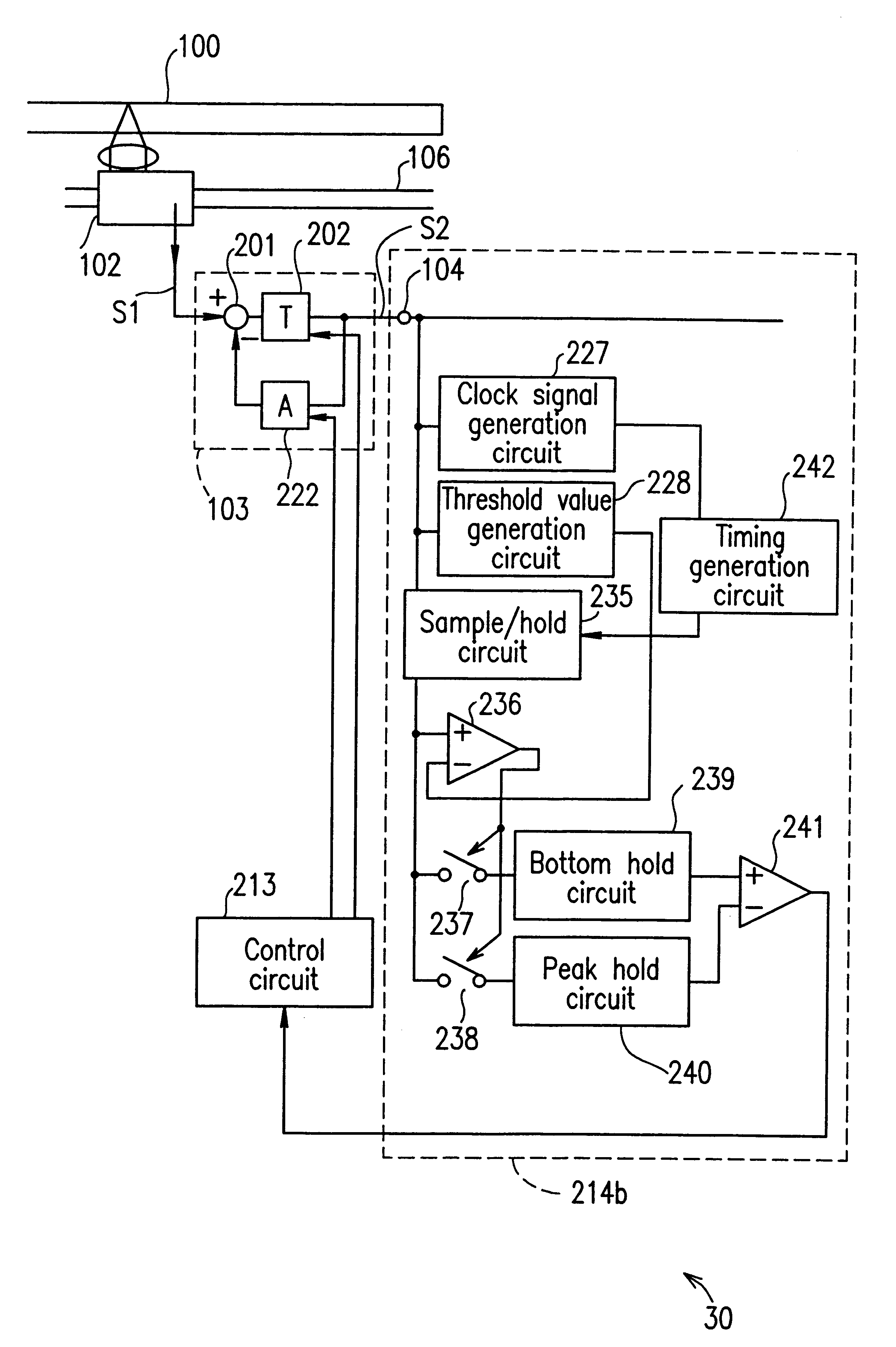
FIG. 14 is a block diagram illustrating an optical information processing apparatus 30 according to Example 3 of the present invention. The optical information processing apparatus 30 optimizes the signal processing circuit 103 so as to maximize the opening of the eye pattern of the reproduction signal S2 output from the signal processing circuit 103. Specifically, the optical information processing apparatus 30 optimizes the delay time T and the gain A so as to maximize the opening of the eye pattern of the reproduction signal S2.

The optical information processing apparatus 30 includes an optical head 102, a transportation member 106, a signal processing circuit 103, a control circuit 213, and an eye opening detection circuit 214.

The eye opening detection circuit 214 rec...

example 4

(Example 4)

FIG. 20 is a block diagram illustrating an optical information processing apparatus 40 according to Example 4 of the present invention. The description of the constituent elements having the same functions as those described in Example 1 is omitted unless necessary.

A reproduction signal S1 which is output from an optical head 102 and input to a signal processing circuit 105 is coupled to a positive input terminal of a differential circuit 201 and a delay circuit 202. The reproduction signal S1 is delayed by a delay time T in the delay circuit 202, and the delayed signal is multiplied by A in an amplifier circuit 203. The multiplied signal is coupled to a negative input terminal of the differential circuit 201. The differential circuit 201 subtracts the signal coupled to its positive input terminal from the signal coupled to its negative input terminal so as to output the result of subtraction at a terminal 104.

The differential circuit 201 and the amplifier circuit 203 sho...


PUM


Abstract

An optical information processing apparatus includes: an optical head for radiating a light beam onto an information storage medium and generating a reproduction signal from the light beam reflected an/or diffracted from the information storage medium, the information storage medium carrying optically readable information recorded thereon; a transportation member for causing a relative movement of the optical head with respect to the information storage medium; and a signal processing circuit for receiving the reproduction signal generated by the optical head and processing the reproduction signal. The reproduction signal obtained from the information storage medium irradiated with the light beam includes first information from a mark near a boundary between a region which is heated by the light beam to no less than a predetermined temperature and a first region which is at a temperature below the predetermined temperature, and second information from a mark near a boundary between the region which is heated to no less than the predetermined temperature and a second region which is at a temperature below the predetermined temperature. The signal processing circuit separates the first information from the second information, or vice versa, thereby obtaining from the reproduction signal the information recorded on the information storage medium.

Description

1. Field of the InventionThe present invention relates to an optical information processing apparatus for recording and reproducing information on an information storage medium capable of optical recording and reproduction of information, e.g., optical disks or optical cards.2. Description of the Related ArtIn the field of optical memory technologies utilizing optical disks or optical cards, there is an increasing variety of applications including digital audio disks, video disks, data files, and the like. According to optical memory technologies, the information on an information storage medium can be reproduced by using a fine beam of light to read minute convex and concave portions, or marks and spaces (which have distinguishable physical properties from each other) provided on the medium.FIG. 22 is a diagram illustrating the relationship between aforementioned marks and a fine light beam, where information is recorded based on differential orientations of magnetization on an opt...

Claims


Application Information

Patent Timeline
IPC IPC(8): G11B11/00G11B11/105G11B7/005G11B7/00G11B11/10
CPCG11B11/10515G11B7/005
Inventor SANO, KOUSEITANAKA, SHIN-ICHIKADOWAKI, SHIN-ICHI
Owner PANASONIC CORP
Why Eureka
Try Eureka