Structure having laser ablated features and method of fabricating

a technology of laser ablation and features, applied in the direction of printed circuit manufacturing, conductive pattern formation, insulation substrate metal adhesion improvement, etc., can solve the problems of large difficulty in adequately etching dendrites, complex and compact requirements of printed boards, and large increase in compactness and electrical performance requirements

Inactive Publication Date: 2005-07-19
META PLATFORMS INC
View PDF27 Cites 150 Cited by
  • Summary
  • Abstract
  • Description
  • Claims
  • Application Information

AI Technical Summary

Benefits of technology

[0007]The present invention provides for obtaining a structure having dense embedded flush circuitry features. The present invention makes it possible to create circuitry features that are much more densely configured than those fabricated using current methods. This is made possible since the final structure is a circuitry feature having dielectric regions and conductive features that are coplanar.

Problems solved by technology

For instance, the complexity, compactness and electrical performance requirements of printed boards have significantly increased over the last several years.
Smooth copper layers do not adequately bond without an auxiliary bonding agent.
Great difficulties exist in adequately etching dendrites especially when dealing with small spaces.
Moreover, along with the concern created by dendrites, the width of the lines (e.g. about 0.5 mils wide), and photolithographic issues (e.g. resolution of fine features, 0.7 mil wire with 1.1 mil space, in a thin photo resist film), and subtractive etch undercut / pad rounding, render clearly and fully resolving small line spaces such as the 1.8 mil pitch features presently desired very difficult.
Additionally, this subtractive etch approach results in unprotected circuitry features referred to as “skyscrapers” that extend above an underlying plane of dielectric barrier material.
The “skyscraper” structure causes a problem of bridging or shorting between lines especially where there exist closely spaced fingers.

Method used


Image

  • Structure having laser ablated features and method of fabricating
  • Structure having laser ablated features and method of fabricating
  • Structure having laser ablated features and method of fabricating

Examples


Embodiment Construction

[0018]In order to facilitate an understanding of the invention, reference will be made to the figures.

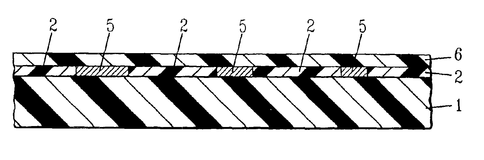
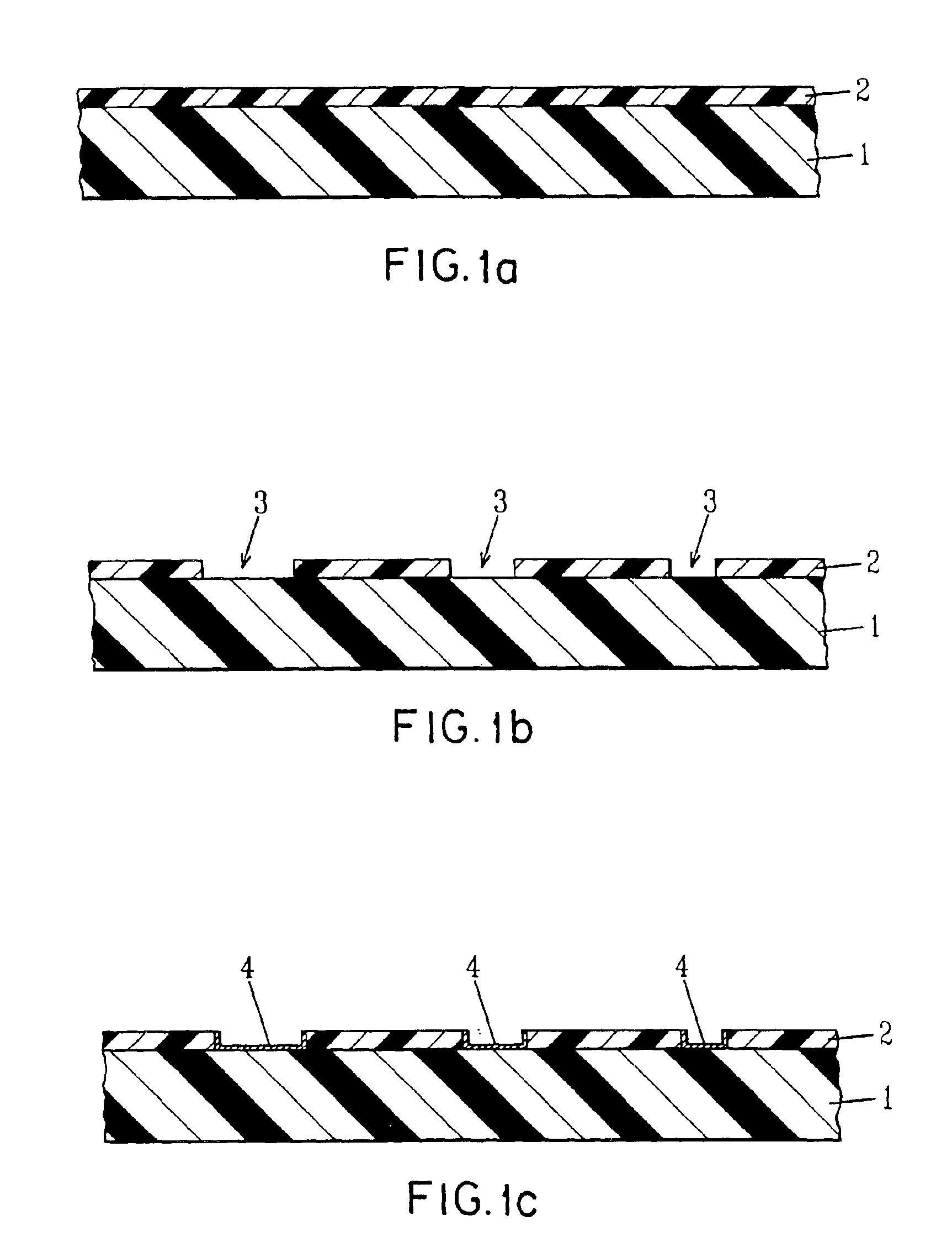
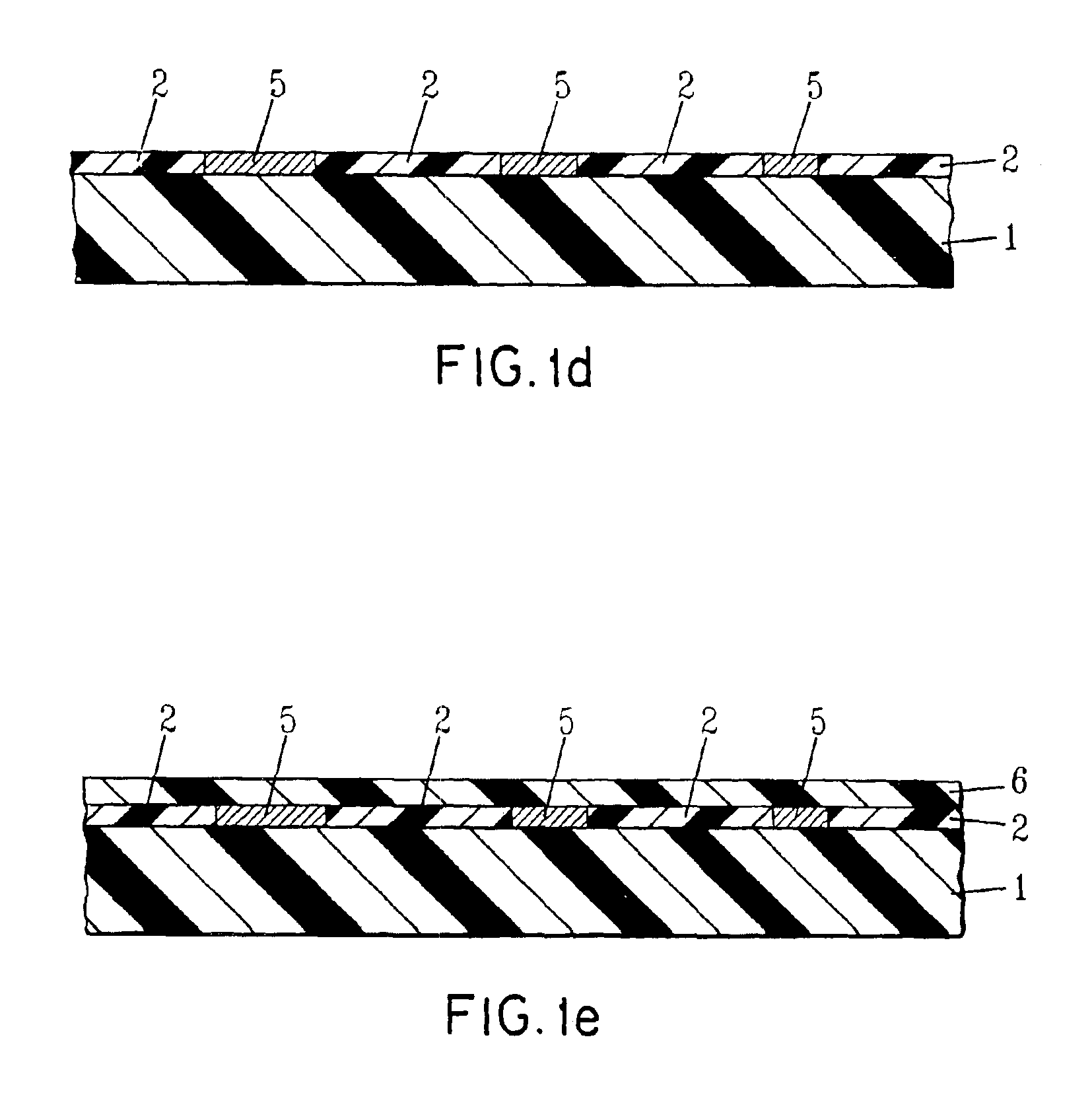
[0019]The structure of the present invention having embedded flush or coplanar circuitry features can be produced by providing a flat, rigid dielectric layer of a first polymeric material (see FIG. 1a).

[0020]The dielectric substrate can be a thermoplastic resin or thermosetting resin. When a thermosetting resin is employed, it is in the uncured or partially cured (B-stage) until after the embedding is completed. At that point, the thermosetting resin can be fully cured.

[0021]Typical thermosetting resins include epoxy resins, polyimides, bis-maleimidetriazine resins, and melamine resins.

[0022]Typical thermoplastic resins include polyamides, polytretrafluoroethylene resins, hexafluoropropylene resin, polyether sulfone resins and polyolefins such as polyethylene and polypropylene.

[0023]The dielectric substrate, if desired, can be reinforced such as with glass fibers or glass fabric.

[00...


PUM

PropertyMeasurementUnit
thickaaaaaaaaaa
thickaaaaaaaaaa
thickaaaaaaaaaa

Abstract

Embedded flush circuitry features are provided by providing a conductive seed layer on the sidewalls and bottom of laser ablated trench features plating a layer of conductive metal onto the seed layer and depositing a layer of dielectric material.

Description

CROSS-REFERENCE TO RELATED APPLICATION[0001]The present application is a continuation of U.S. patent application Ser. No. 09 / 804,921 filed Mar. 13, 2001, now U.S. Pat. No. 6,730,857.FIELD OF THE INVENTION[0002]The present invention relates to providing a structure having circuitry features and in particular to embedded flush circuitry features. The present invention is especially advantageous for fabricating buried interconnection levels that are in close proximity to one another in a printed circuit board structure.BACKGROUND OF THE INVENTION[0003]Printed circuit boards find a wide variety of uses in the electronics industry with the demand for high performance, printed wiring, or circuit boards for various applications steadily increasing. For instance, the complexity, compactness and electrical performance requirements of printed boards have significantly increased over the last several years. The demands on printed circuit boards require high density packaging, fine interconnect...

Claims


Application Information

Patent Timeline
Patent Type & Authority Patents(United States)
IPC IPC(8): H05K3/46H05K3/02H05K3/00H05K3/10H05K3/04H05K3/38H05K3/18
CPCH05K3/465H05K3/0032H05K3/045H05K3/107H05K3/184H05K3/388Y10T29/49124H05K3/4661H05K2203/072H05K2203/107H05K2203/1338
Inventor KONRAD, JOHN JOSEPHMCKEVENY, JEFFREYWILSON, JAMES WARREN
Owner META PLATFORMS INC
Why Eureka
Try Eureka