Gate-coupled MOSFET ESD protection circuit

Inactive Publication Date: 2005-07-19
WINBOND ELECTRONICS CORP
View PDF2 Cites 79 Cited by
  • Summary
  • Abstract
  • Description
  • Claims
  • Application Information

AI Technical Summary

Benefits of technology

[0021]Thus, in the present invention, the device size is smaller than that of the conventional voltage-clamping ESD protection

Problems solved by technology

However, certain concerns are that (i) the device size is typically very large, e.g., with a number of power-bus-clamp NMOSFETs having a total channel width of 4000 to 10,000 m; and (ii) the inverter 11 amplifies the power-bus noise through the node E, causing un

Method used


Image

  • Gate-coupled MOSFET ESD protection circuit
  • Gate-coupled MOSFET ESD protection circuit
  • Gate-coupled MOSFET ESD protection circuit

Examples


Example

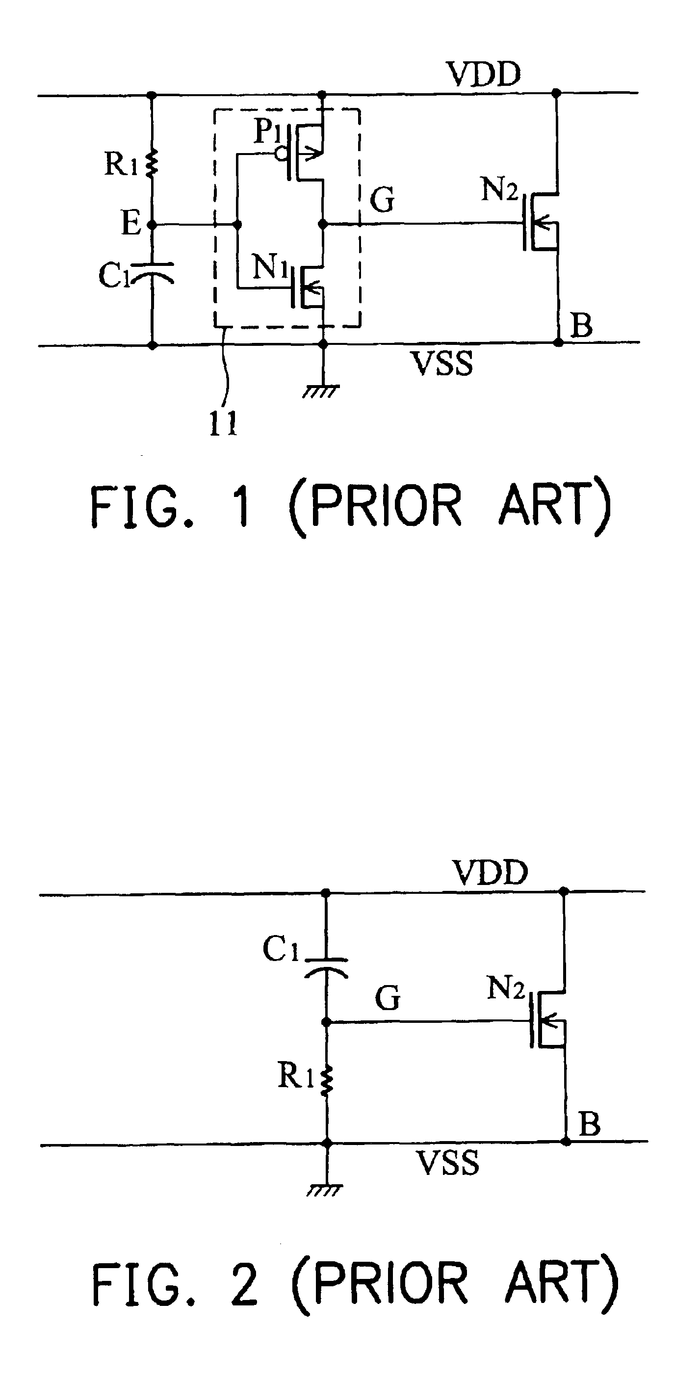
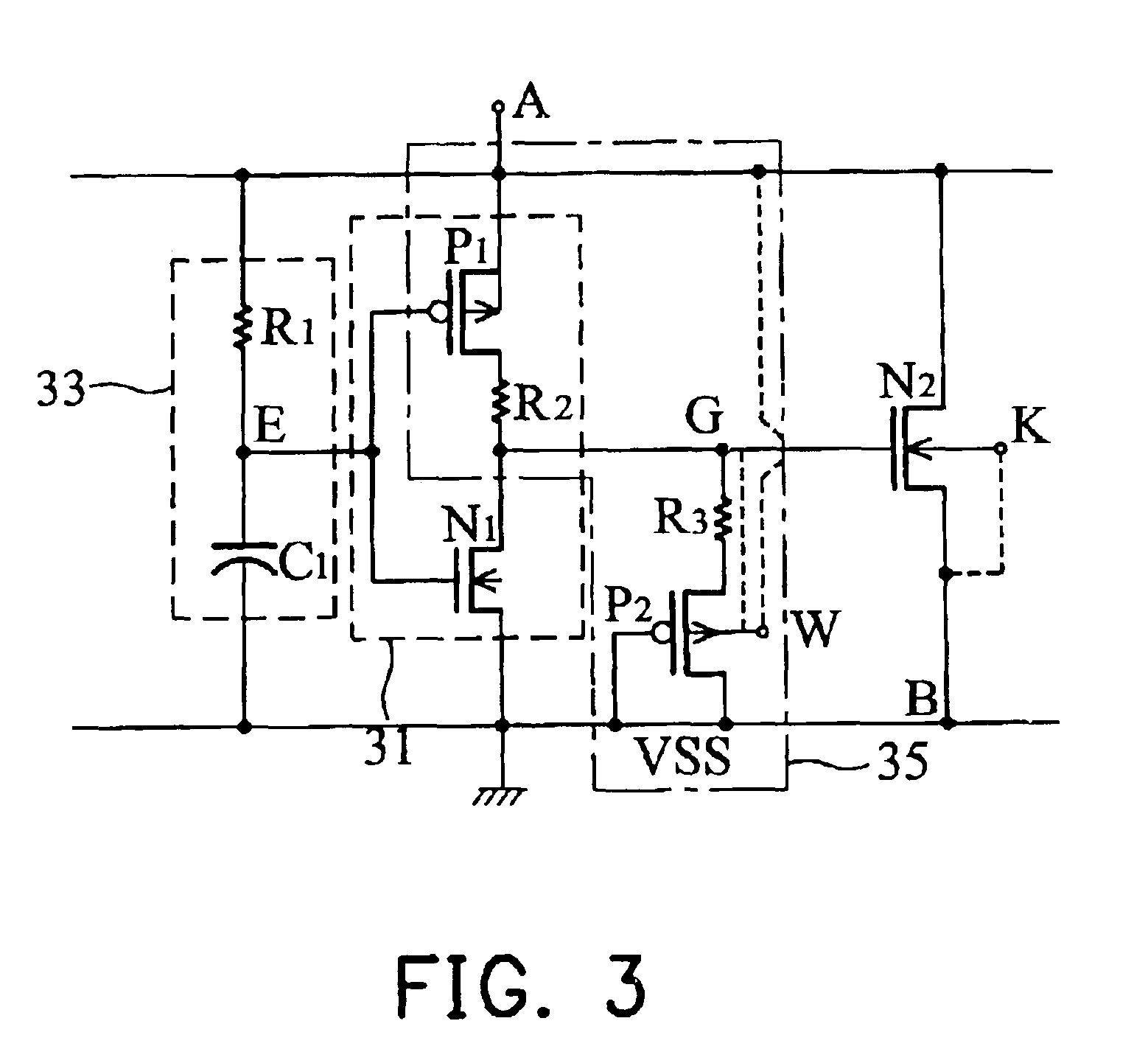
[0033]FIG. 3 is a diagram showing an ESD protection circuit according to a first embodiment of the invention. A gate-coupled MOSFET ESD protection circuit provides an ESD path from a node A to node B when an ESD pulse voltage applied to the node A. The circuit comprises a timing-control circuit 33 composed of a resistor R1 and a capacitor C1, a voltage divider 35 composed of transistors P1 and P2 and resistors R2 and R3, and a N type shunt transistor N2. The timing-control circuit 33 outputs a low voltage at the node E when the ESD pulse voltage is applied to the node A. The voltage divider 35 outputs a voltage divided from the ESD voltage at the node G when activated by the low voltage output from the timing-control circuit 33. The shunt transistor N2 has a drain coupled to the node A, a source coupled to the node B and a gate coupled to the voltage divider 35, and enters into a snapback to provide the ESD path by the drain and gate receiving the ESD and the voltage at node G when ...

Example

[0041]FIG. 4A is a diagram showing an ESD protection circuit according to a second embodiment of the invention. This is an alternative circuit modified from the one shown in FIG. 3. The transistor P2 is replaced by the resistor R3 and the transistor N1 is removed. The voltage dividing ratio is

VG / VA=R3 / [RON(P1)+R2+R3]

which is preferably from {fraction (1 / 15)} to ⅗ so that the gate voltage of the transistor N2 can range from 1 to 2 volts, 0.5 to 2.5 volts or 0.5V to half of the voltage at the node A.

Example

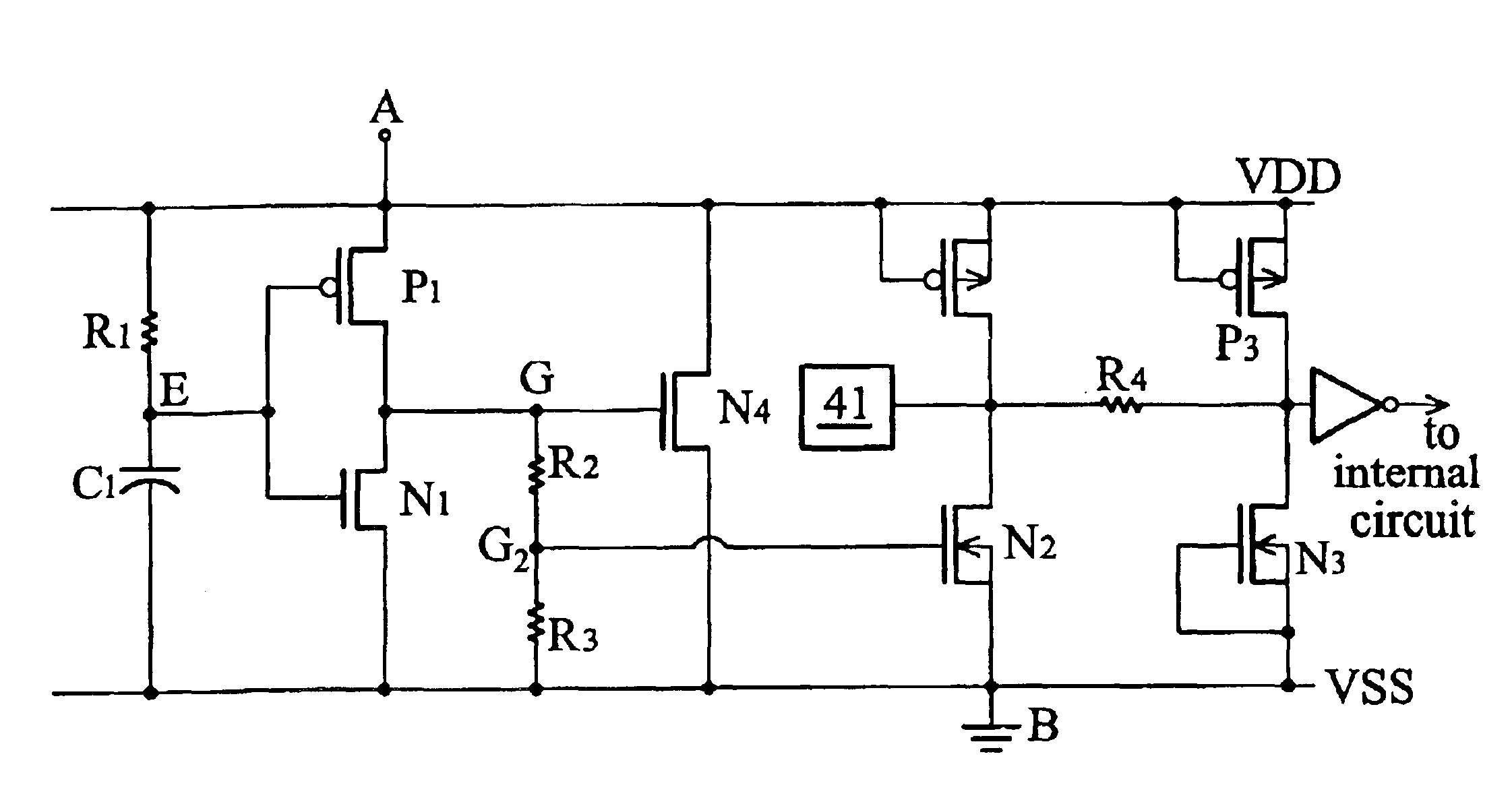
[0042]FIG. 4B is a diagram showing an ESD protection circuit according to a third embodiment of the invention. This is an ESD protection circuit providing ESD paths from more than one node (IC pins or power bus) to the VSS power bus. When the ESD event occurs, the transistor N2 provides an ESD path from the pad to the VSS power bus by entering into the snapback while the transistor N4 provides an ESD path from the VDD to the VSS power bus by being turned on.

[0043]When a positive ESD event occurs on the VDD power bus, the ESD pulse voltage is divided by the voltage divider with a voltage-dividing ratio of VG1 / VA=[R2+R3] / [RON(P1)+R2+R3], received by the gate of the transistor N4 and directly turns on the transistor N4. When a positive ESD event occurs on the pad, the ESD pulse voltage is coupled to the VDD power bus, which turns on the transistor N4 and applies a voltage divided from the ESDF pulse voltage with a ratio of VG2 / VA=[R3] / [RON(P1)+R2+R3]. This reduces the triggering voltag...


PUM


Abstract

A gate-coupled MOSFET ESD protection circuit. The circuit has a gate-node potential controlled by an inverter and a timing control circuit. Unlike current-shunting ESD clamping devices that turn the MOSFET fully on during an ESD event, a pull-down element is included to form a voltage divider like circuit, such that the gate-node potential is limited to around 1 to 2 volts during a positive ESD transient event. Unlike GCNMOS (Gate-Coupled NMOS), the invention has better control of the transient gate potential for more effective triggering of the NMOS into snapback during an ESD event.

Description

[0001]Pursuant to 35 U.S.C. § 119(a)-(d), this application claims priority from Taiwanese application no. 91109035, filed on April 30,2002.BACKGROUND OF THE INVENTION[0002]1. Field of the Invention[0003]The present invention relates to an ESD protection circuit and particularly to a gate-coupled MOSFET ESD protection circuit.[0004]2. Description of the Prior Art[0005]In a Human-Body-Model ESD transient, a 100PF capacitor is first charged up to an ESD pulse voltage, and then discharged through a 1.5-kohm resistor onto an IC pin. Typically, a pulse voltage level of 2 KV is used to qualify an IC package. The initial peak current is roughly 1.2 A with a rise time of approximately 10 nsec. For integrated circuit packages, the VDD-to-VSS capacitance is typically larger than 1 NF. If the ESD energy is directly absorbed by the power bus (for ESD stress of VDD pin to VSS pin), or indirectly absorbed by the power bus (for example, positive ESD stress on an input or I / O pin that has a pull up ...

Claims


Application Information

Patent Timeline
IPC IPC(8): H01L29/74H01L23/58H01L23/62H01L29/66H02H9/00H01L27/02
CPCH01L27/0266H01L2924/0002H01L2924/00
Inventor LIN, SHI-TRONCHEN, WEI-FAN
Owner WINBOND ELECTRONICS CORP
Why Eureka
Try Eureka