Plating method and apparatus for controlling deposition on predetermined portions of a workpiece

a technology of predetermined portions and workpieces, applied in the direction of resistive material coating, solid-state device, metallic material coating process, etc., can solve the problems of voids, defects such as seams and voids, and the molecules cannot effectively diffuse to the bottom surface of high aspect ratio features. , to achieve the effect of minimizing the amount of time and superior quality

Inactive Publication Date: 2005-07-26
NOVELLUS SYSTEMS
View PDF6 Cites 31 Cited by
  • Summary
  • Abstract
  • Description
  • Claims
  • Application Information

AI Technical Summary

Benefits of technology

[0023]It is another object of the present invention to provide apparatus and methods that plate a conductive material in both small and large features of a workpiece surface with efficiency, cost-savings, and superior quality.
[0024]It is a further object of the present invention to provide apparatus and methods for using a workpiece surface influencing device to obtain a differential between additives disposed on a top surface of a conductive layer and additives within cavity surfaces of the conductive layer, while minimizing the surface area of the workpiece surface influencing device that contacts the top surface of the conductive layer.
[0025]It is a further object of the present invention to provide apparatus and methods for using a workpiece surface influencing device to obtain a differential between additives disposed on a top surface of a conductive layer and additives within cavity surfaces of the conductive layer, while minimizing the amount of time that the workpiece surface influencing device contacts a given area on the top surface of the conductive layer.

Problems solved by technology

Copper does not completely fill the trench 4e because the additives that are used in the bath formulation are not operative in large features.
These molecules cannot effectively diffuse to the bottom surface of the high aspect ratio features such as the vias of FIG.
Without the appropriate additives, Cu can grow on the vertical walls as well as the bottom surface of the high aspect ratio features at the same rate, thereby causing defects such as seams and voids, as is well known in the industry.
In reality these material removal processes are known to be quite costly and problematic.
First of all, removal of a thick Cu layer is time consuming and costly.
Secondly, the non-uniform surface cannot be removed uniformly and results in dishing defects in large features as well known in the industry and as shown in FIG. 2e.
This is necessary because, as mentioned above, lack of bottom-up filling can cause defects in the small features.

Method used


Image

  • Plating method and apparatus for controlling deposition on predetermined portions of a workpiece
  • Plating method and apparatus for controlling deposition on predetermined portions of a workpiece
  • Plating method and apparatus for controlling deposition on predetermined portions of a workpiece

Examples


Embodiment Construction

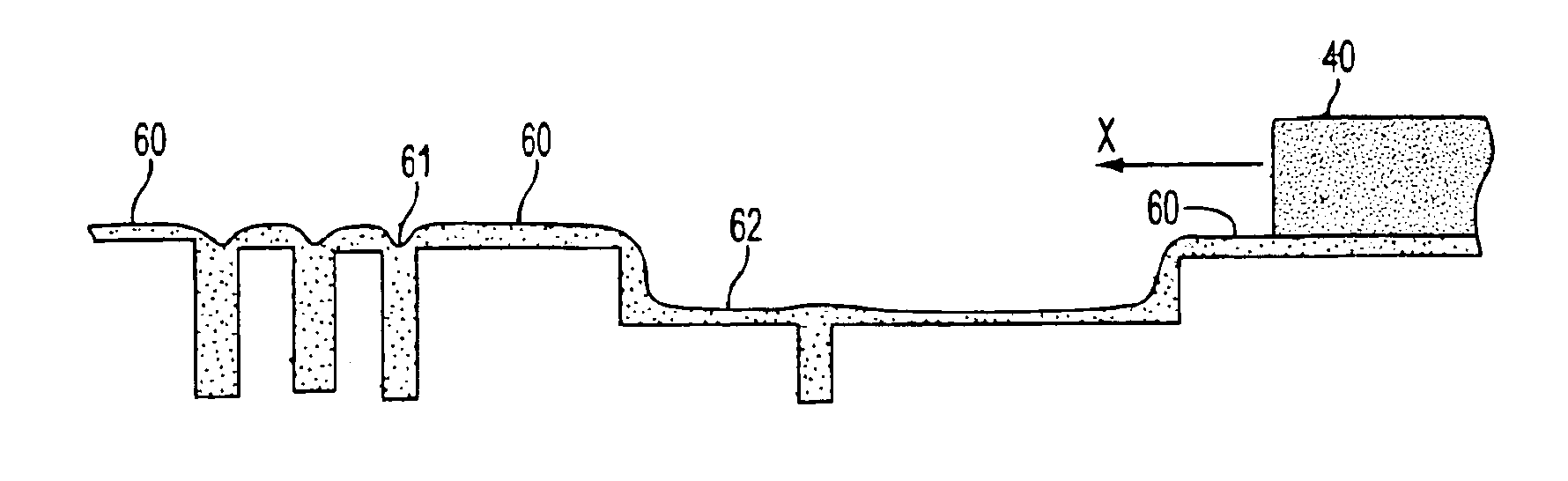
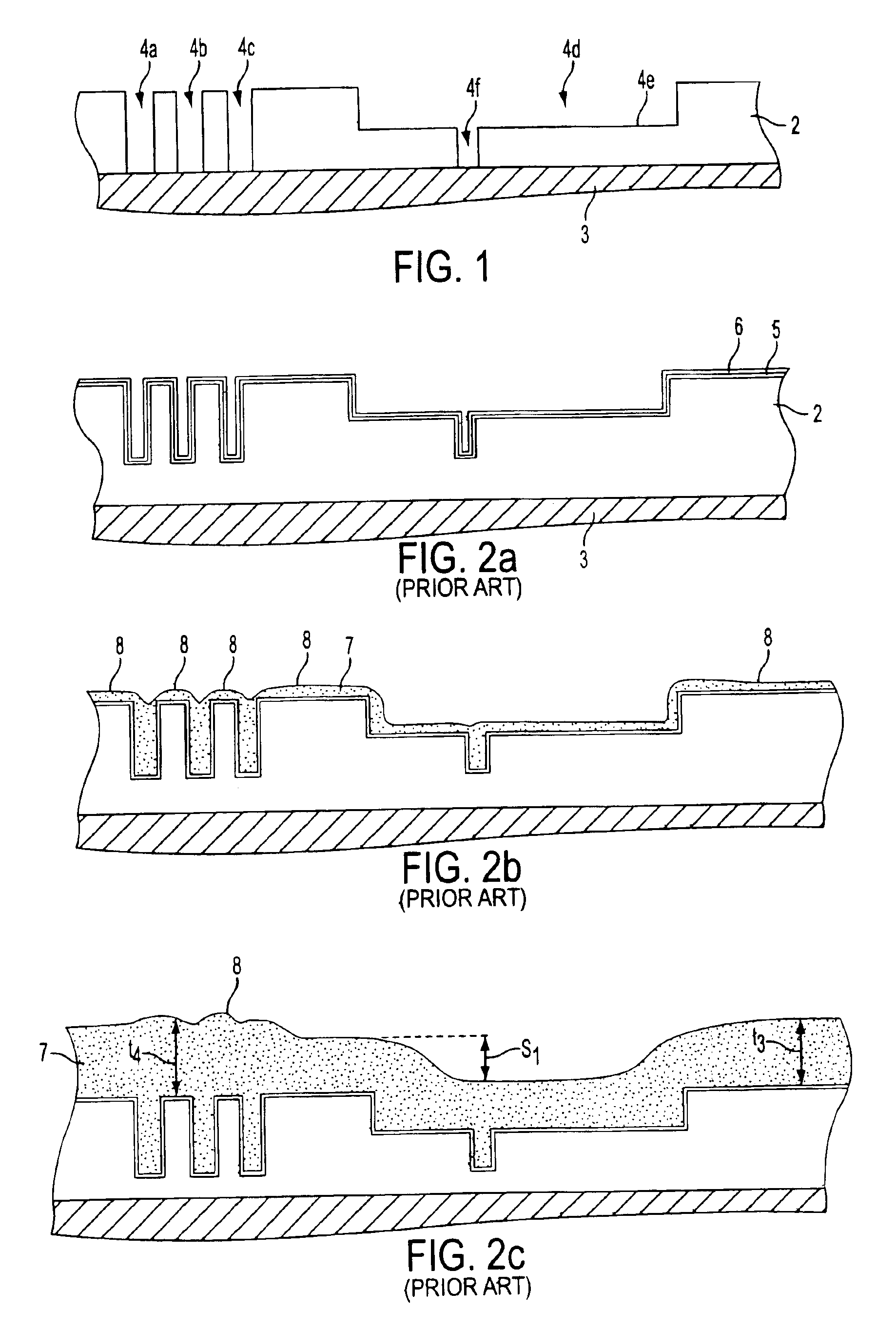
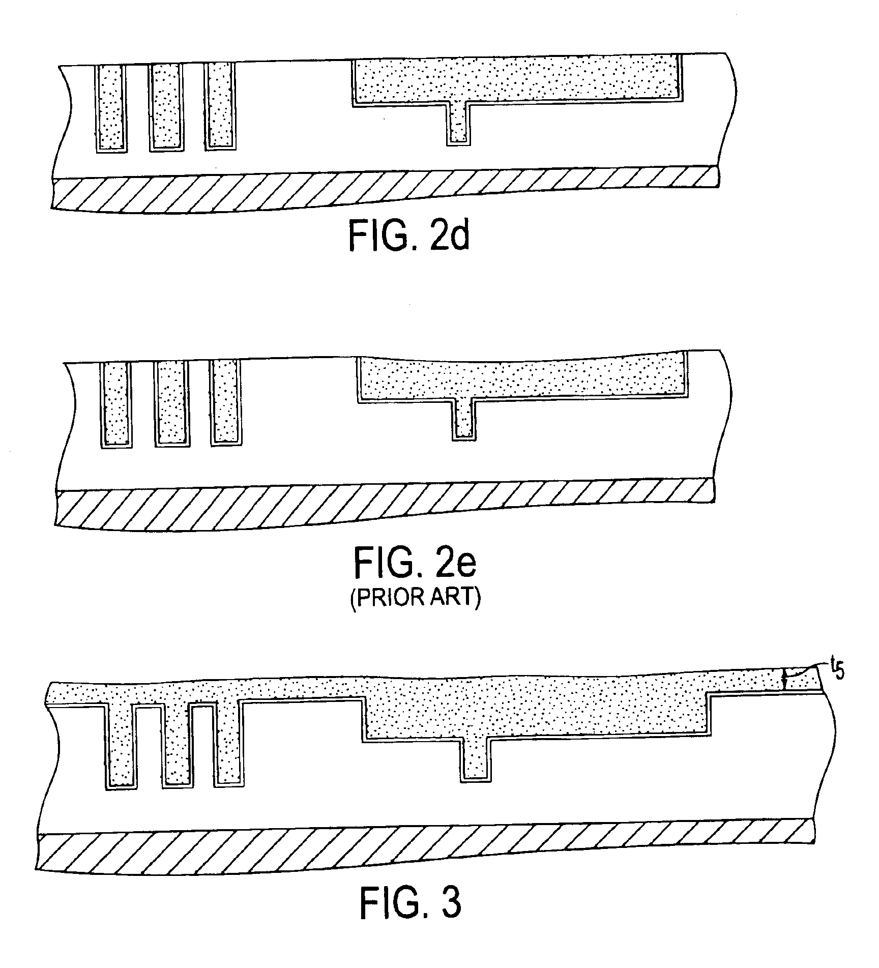
[0044]The preferred embodiments of the present invention will now be described with reference to the following figures. The inventors of the present invention have found that by plating the conductive material on the workpiece surface using the present invention, a more desirable and high quality conductive material can be deposited in the various features therein.

[0045]The present invention can be used with any workpiece such as a semiconductor wafer, flat panel, magnetic film head, packaging substrate, and the like. Further, specific processing parameters such as material, time and pressure, and the like are provided herein, which specific parameters are intended to be explanatory rather than limiting. For example, although copper is given as an example of the plated material, any other material can be electroplated using this invention provided that the plating solution has at least one of plating enhancing and inhibiting additives in it.

[0046]The plating method described herein ...


PUM

PropertyMeasurementUnit
surface areaaaaaaaaaaa

Abstract

The present invention relates to methods and apparatus for plating a conductive material on a workpiece surface in a highly desirable manner. Using a workpiece-surface-influencing device, such as a mask or sweeper, that preferentially contacts the top surface of the workpiece, relative movement between the workpiece and the workpiece-surface-influencing device is established so that an additive in the electrolyte solution disposed on the workpiece and which is adsorbed onto the top surface is removed or otherwise its amount or concentration changed with respect to the additive on the cavity surface of the workpiece. Plating of the conductive material can place prior to, during and after usage of the workpiece-surface-influencing device, particularly after the workpiece surface influencing device no longer contacts any portion of the top surface of the workpiece, to achieve desirable semiconductor structures.

Description

CROSS-REFERENCE TO RELATED APPLICATIONS[0001]This application is a continuation-in-part of and claims the benefit of priority under 35 USC 119 / 120 to the following:[0002]application Ser. No. 09 / 919,788 filed Jul. 31, 2001 entitled Plating Method and Apparatus that Creates A Differential Between Additive Disposed on a Top Surface and a Cavity Surface of a Workpiece Using an Indirect External Influence, now U.S. Pat. No. 6,858,121, which is a continuation-in-part of:[0003]application Ser. No. 09 / 740,701 filed Dec. 18, 2000 entitled Plating Method and Apparatus that Creates A Differential Between Additive Disposed on a Top Surface and a Cavity Surface of a Workpiece Using an External Influence, now U.S. Pat. No. 6,534,116,[0004]all of which claim the benefit of priority to Provisional Application Ser. No. 60 / 224,739 filed Aug. 10, 2000 entitled Masked Pulse Plating Method and Apparatus.FIELD OF THE INVENTION[0005]The present invention relates generally to an electroplating method and a...

Claims


Application Information

Patent Timeline
Patent Type & Authority Patents(United States)
IPC IPC(8): C25D5/22C25D5/00C25D5/34H01L21/288H01L21/02H01L21/768H01L21/70C25D5/02C25D5/08C25D5/18C25D7/12C25D17/00C25D21/00H01L21/3205H01L23/12
CPCC25D5/06C25D5/10C25D5/22C25D5/34H01L21/2885H01L21/76877H01L21/76879C25D7/123C25D17/001H01L21/7684Y10T428/24562C25D5/611
Inventor BASOL, BULENT M.
Owner NOVELLUS SYSTEMS
Why Eureka
Try Eureka