Systems and methods for simultaneous or sequential multi-perspective specimen defect inspection

a technology of system and method, applied in the direction of semiconductor/solid-state device testing/measurement, instruments, material analysis, etc., can solve the problems of not being very effective for other defect types such as scratches, complicating specimen inspection, and detecting a larger range of defects, so as to reduce unwanted diffraction orders, and reduce the diameter of the second beam

Inactive Publication Date: 2005-07-26
KLA TENCOR TECH CORP
View PDF15 Cites 38 Cited by
  • Summary
  • Abstract
  • Description
  • Claims
  • Application Information

AI Technical Summary

Benefits of technology

[0009]Inspecting specimens such as wafers may be complicated due to, for example, the variety of defects that may need to be detected and a diverse array of background circuitry against which the detection may be performed. Generally, in light scattering systems, for example, a given illumination / collection strategy may be substantially optimized for one category of defects such as particles but may not be very effective for other defect types such as scratches. In this manner, a light scattering system that includes a plurality of illumination / collection systems, each of which, operated simultaneously or sequentially, may have good sensitivity for different defect types. As such, a dual incidence illumination system may detect a larger range of defects than a single incidence system.
[0010]A dual incidence illumination system may include, for example, a normal incidence illumination channel and an oblique illumination channel. Such a system may provide uniform scratch sensitivity, as well as the potential for a versatile bright field, excellent pattern defect inspection, background pattern suppression, and foreign particle detection capability. Inspecting a specimen may involve using only one of the plurality of illumination / collection system depending on, for example, a specific application of the inspection. In addition, illumination may vary from site to site across a surface of a specimen. For such illumination, a spot size of a normal incidence beam may be approximately equal to a spot size of an oblique incidence beam. In addition, scanning of the normal incidence beam and the oblique incidence beam may be synchronized for such illumination. Because the illumination / collection systems may operate simultaneously, however, a throughput of such an inspection system may not be reduced due to using additional illumination / collection systems for inspecting a specimen. In addition, such a light scattering system may provide a capability for fast classification of the defects.
[0018]In an embodiment, illuminating the surface of the specimen may include reducing a diameter of the second beam of light in one direction such that a shape of the second beam of light incident on the surface of the specimen is substantially the same as a shape of the first beam of light incident on the surface of the specimen. Illuminating the surface of the specimen may include increasing a telecentricity of the second beam of light with a focusing lens in a non-telecentric geometry positioned in a path of the second beam of light. Illuminating the surface of the specimen may include illuminating the surface of the specimen with an illumination system arranged in a Mach-Zehnder type arrangement.
[0019]In an embodiment, the method may also include collecting at least a portion of the first and second beams of light returned from the surface of the specimen. Collecting at least the portion of the first beam of light may include collecting the first beam of light with at least one collector. At least the one collector may include a single dark field collector, a double dark field collector, a near normal dark field collector, or any combination thereof. Collecting at least the portion of the second beam of light may include collecting the second beam of light with at least one collector. At least the one collector may include a single dark field collector, a near normal dark field collector, a bright field collector, or any combination thereof. The method may also include reducing unwanted diffraction orders in the first beam of light scattered from the surface of the specimen and reducing unwanted diffraction orders in the second beam of light scattered from the surface of the specimen.

Problems solved by technology

Inspecting specimens such as wafers may be complicated due to, for example, the variety of defects that may need to be detected and a diverse array of background circuitry against which the detection may be performed.
Generally, in light scattering systems, for example, a given illumination / collection strategy may be substantially optimized for one category of defects such as particles but may not be very effective for other defect types such as scratches.
As such, a dual incidence illumination system may detect a larger range of defects than a single incidence system.
Because the illumination / collection systems may operate simultaneously, however, a throughput of such an inspection system may not be reduced due to using additional illumination / collection systems for inspecting a specimen.

Method used


Image

  • Systems and methods for simultaneous or sequential multi-perspective specimen defect inspection
  • Systems and methods for simultaneous or sequential multi-perspective specimen defect inspection
  • Systems and methods for simultaneous or sequential multi-perspective specimen defect inspection

Examples


Embodiment Construction

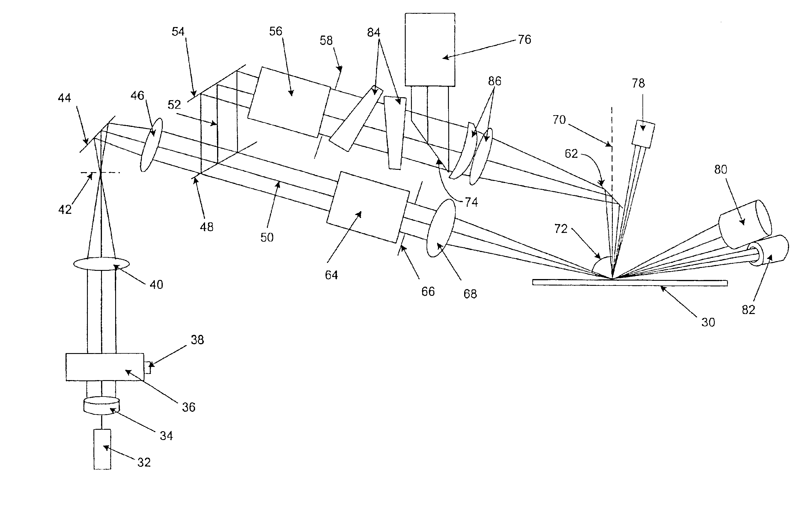
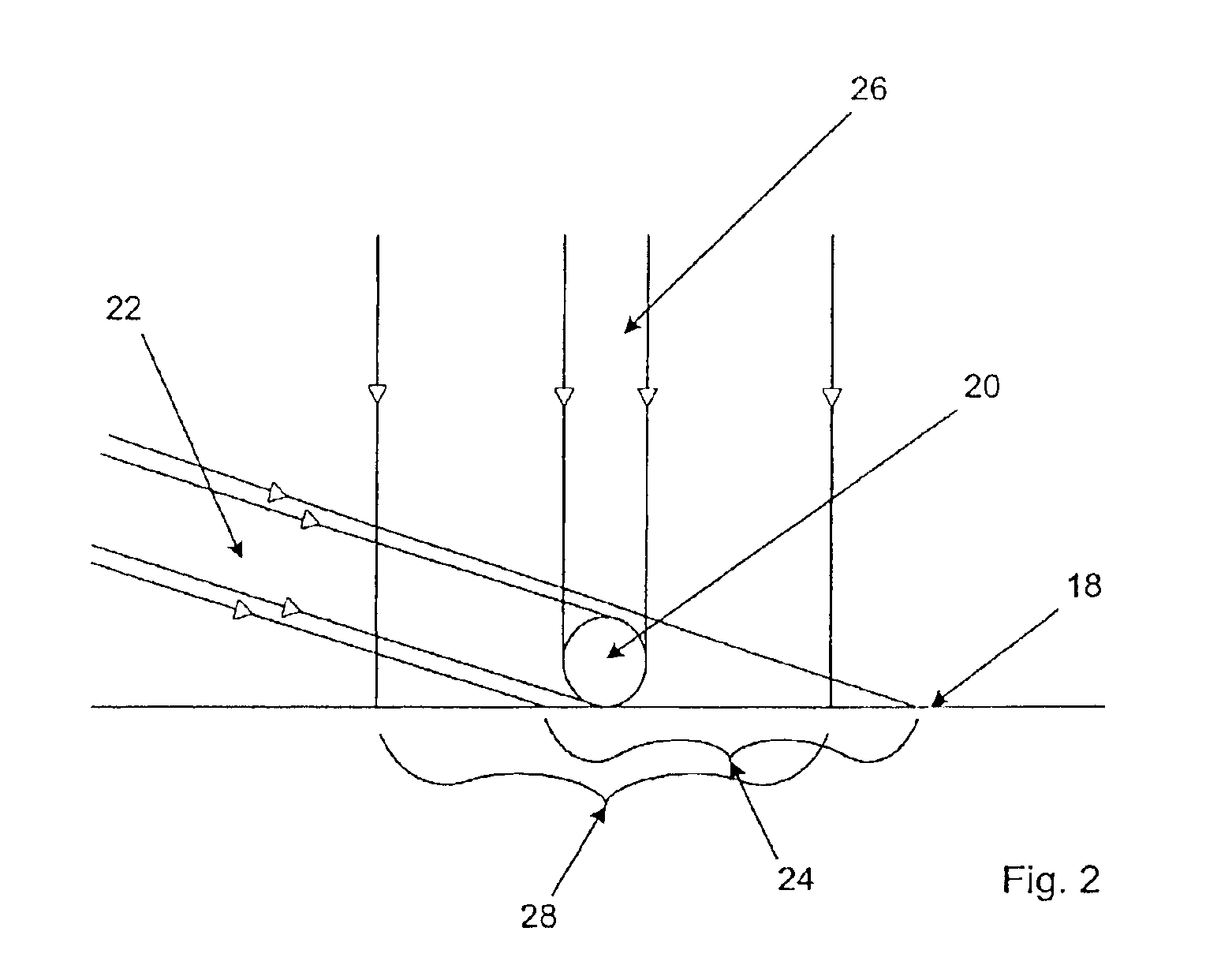
[0029]Inspection system geometries typically fall into three main categories: bright field, single dark field, and double-dark field. “Bright field” generally refers to a collection geometry configured to collect specularly reflected light from an object. A bright field collection geometry may have any angle of incidence although typically it may have an angle of incidence normal to the object plane.

[0030]“Dark field” generally refers to a collection geometry configured to collect only scattered light from an object. The term, however, may also have an additional meaning associated with a surface electromagnetic (“E-M”) field of an object. When an incident E-M field has a high reflection coefficient from a surface, approximate cancellation of the incident and reflected waves may produce a reduced E-M field at the surface, which may be commonly referred to as “dark fringe.” Similarly, the scattered wave and its reflection can constructively or destructively interfere in the far field...


PUM

PropertyMeasurementUnit
angle of incidenceaaaaaaaaaa

Abstract

Systems and methods for inspecting a surface of a specimen such as a semiconductor wafer are provided. A system may include an illumination system configured to direct a first beam of light to a surface of the specimen at an oblique angle of incidence and to direct a second beam of light to a surface of the specimen at a substantially normal angle. The system may also include a collection system configured to collect at least a portion of the first and second beams of light returned from the surface of the specimen. In addition, the system may include a detection system. The detection system may be configured to process the collected portions of the first and second beams of light. In this manner, a presence of defects on the specimen may be detected from the collected portions of the first and second beams of light.

Description

PRIORITY CLAIM[0001]This application claims priority to U.S. Provisional Application No. 60 / 304,480 entitled “Systems and Methods for Simultaneous or Sequential Multi-Perspective Specimen Defect Inspection,” filed Jul. 10, 2001.BACKGROUND OF THE INVENTION[0002]1. Field of the Invention[0003]The present invention generally relates to systems and methods for inspecting a specimen. Certain embodiments relate to systems and methods that include inspecting a specimen with simultaneous or sequential multi-angle illumination.[0004]2. Description of the Relevant Art[0005]Fabricating semiconductor devices such as logic and memory devices may typically include processing a specimen such as a semiconductor wafer using a number of semiconductor fabrication processes to form various features and multiple levels of the semiconductor devices. For example, lithography is a semiconductor fabrication process that typically involves transferring a pattern to a resist arranged on a semiconductor wafer....

Claims


Application Information

Patent Timeline
Patent Type & Authority Patents(United States)
IPC IPC(8): G01N21/47G01N21/88G01N21/95G01N21/94G01N21/84G01N21/956H01L21/027H01L21/66
CPCG01N21/47G01N21/9501G01N21/94G01N2021/8825
Inventor VAEZ-IRAVANI, MEHDISTOKOWSKI, STANBIELLAK, STEVENSULLIVAN, JAMIEWELLS, KEITHNIKOONAHAD, MEHRDAD
Owner KLA TENCOR TECH CORP
Why Eureka
Try Eureka