Control system for a semiconductor laser

a control system and laser technology, applied in the field of lasers, can solve the problems of waste of space, large constraints on the geometry and dimensions of the laser package on which the laser is mounted, and the cost of a laser module is the size of the package, so as to simplify the control method of the laser, reduce the number of components, and reduce the cost

Inactive Publication Date: 2005-07-26
THORNTON ROBERT L
View PDF33 Cites 34 Cited by
  • Summary
  • Abstract
  • Description
  • Claims
  • Application Information

AI Technical Summary

Benefits of technology

[0007]In view of the above, it would be desirable to have some method of increasing the number of independent data items transmitted between the laser and its control circuit, without increasing the number of electrical pins exiting the laser package. Furthermore, it would be desirable to simplify the method of controlling of a laser to operate in a stable manner with a reduced number of components, or with simpler, less expensive components.
[0008]Generally, the present invention relates to a control system architecture that allows a semiconductor laser to be stabilized with respect to critical parameters, such as output power and / or emission wavelength, with a reduced cost with respect to the components required to implement control, while simultaneously maintaining or increasing precision of the control function. This is achieved by using low cost but sophisticated integrated circuitry that is contained within the laser package to measure data related to multiple laser operational parameters and to transmit these parameters to a control circuit. In particular, precision thermal measurements may be used to eliminate the need for optical detectors in the laser package. The invention described herein has significant utility for different types of semiconductor lasers, including both edge emitting and VCSEL-type semiconductor lasers.
[0012]Another embodiment of the invention is directed to a method for controlling an external cavity, vertical cavity, surface emitting laser (EC VCSEL). The EC VCSEL has a cavity formed by a first reflector, an intracavity reflector and an output coupler. The method includes determining a temperature of the cavity of the EC VCSEL and controlling independently the temperature of the cavity of the EC VCSEL to a target value and the bias current of the EC VCSEL so as to maintain laser oscillation on a stable single mode.

Problems solved by technology

The placement of a photodetector at the rear of the laser places significant constraints on the geometry and dimensions of the laser package that the laser is mounted within.
This multiplicity of electrical pins is wasteful of space.
One of the primary drivers for the cost of a laser module is the size of the package, which is in turn driven, in part, by the number of independent electrical connections required to exit the laser package.

Method used


Image

  • Control system for a semiconductor laser
  • Control system for a semiconductor laser
  • Control system for a semiconductor laser

Examples


Embodiment Construction

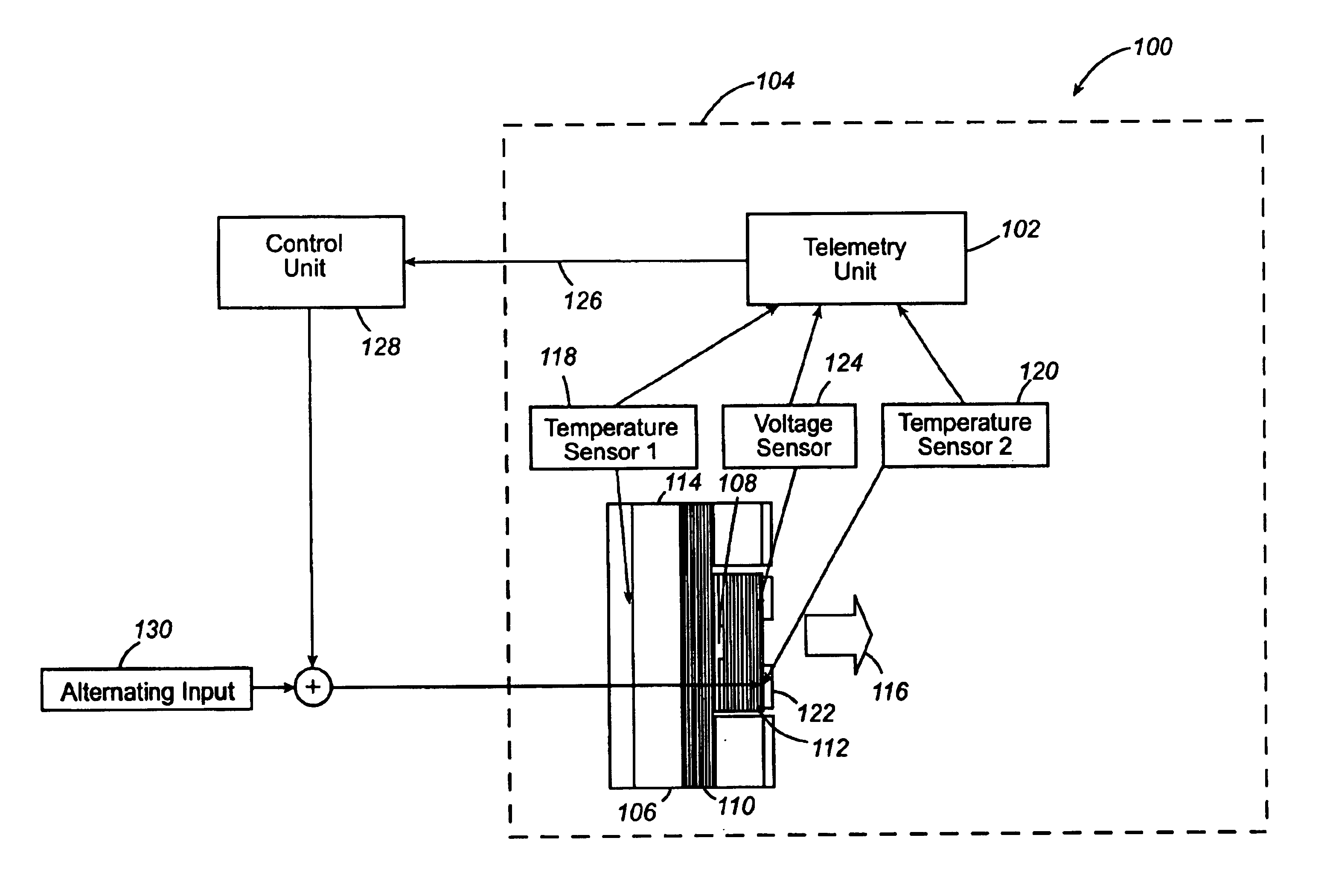
[0026]In general, the present invention is directed to an approach to applying conventional control functionality to a semiconductor laser in a simplified package, and to applying complex control functionality to a semiconductor laser with reduced package complexity. The inclusion of telemetry processing electronics within the laser package itself reduces the need for the multiplicity of output pins when measuring several operating parameters. Consequently, the laser package can be made smaller and less expensive than current approaches, or may remain at the same size, while providing for more sophisticated control algorithms based on a larger set of sense variables. While the invention is applicable to all types of semiconductor lasers, the following description is directed mostly to VCSEL devices, for the purposes of illustration.

[0027]A conventional laser package typically includes a monitoring photodiode for feeding output power information back to the control circuit, and may a...


PUM


Abstract

A control system architecture that allows a semiconductor laser to be stabilized with respect to critical parameters, such as output power and / or emission wavelength, with a reduced cost with respect to the components required to implement control, while simultaneously maintaining or increasing precision of the control function. This is achieved using sophisticated integrated circuitry contained within the laser package to measure data related to multiple laser operation parameters and to transmit these parameters to a control circuit. In particular, precision thermal measurements may be used to eliminate the need for optical detectors in the laser package. The invention described herein has significant utility for different types of semiconductor lasers, including both edge emitting and VCSEL-type semiconductor lasers.

Description

FIELD OF THE INVENTION[0001]The present invention is directed generally to lasers, and more particularly to an approach to packaging and controlling a semiconductor laser.BACKGROUND[0002]Semiconductor lasers are key elements in the advancing performance of many systems, such as optical fiber communications, optical data storage, laser printing, optical clock generation and quantum key distribution. It is almost always the case that to achieve a high level of system performance, the emission characteristics of the laser must be maintained within a well-defined, and typically relatively narrow, window. In the most common and simplest cases, this window is defined to be an output power level window, and an optical photodetector is used to monitor and control the output power level from the device.[0003]For edge emitting, semiconductor lasers, the power is typically monitored from the emission from the rear facet of the laser, while the useful power is extracted from the front facet. Th...

Claims


Application Information

Patent Timeline
Patent Type & Authority Patents(United States)
IPC IPC(8): H01S3/13H01S3/10H01S3/00H01SH01S5/026H01S5/068H01S5/18H01S5/183
CPCH01S5/026H01S5/06804H01S5/02284H01S5/0427H01S5/06258H01S5/146H01S5/06808H01S5/141H01S5/183H01S5/18305H01S5/02251
Inventor THORNTON, ROBERT L.
Owner THORNTON ROBERT L
Why Eureka
Try Eureka