
MEMS driver circuit arrangement

a driver circuit and driver technology, applied in the field of optical systems, can solve the problems of high system cost, system level significant drawbacks, and need to replace the entire device, so as to reduce thermal problems, avoid the training of the overall system, and increase the overall functionality

Inactive Publication Date: 2005-07-26
LUCENT TECH INC +1
View PDF3 Cites 13 Cited by
  • Summary
  • Abstract
  • Description
  • Claims
  • Application Information

AI Technical Summary

Benefits of technology

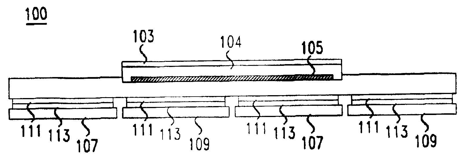
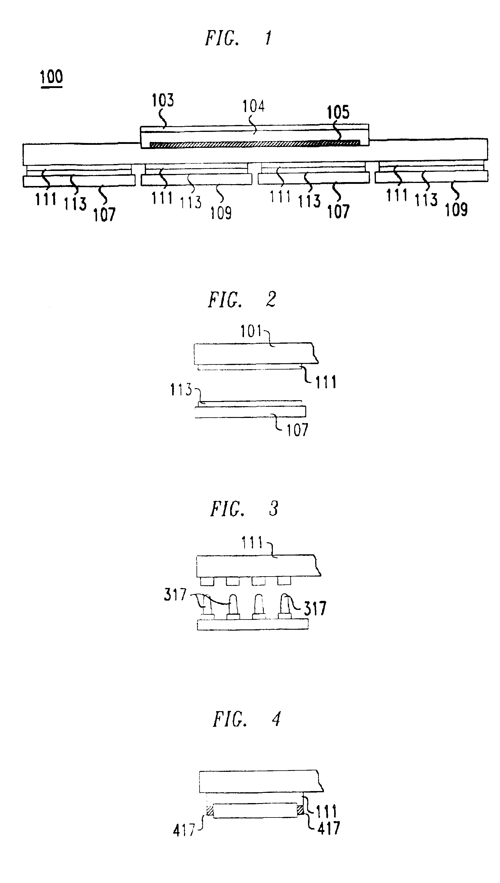
"The patent text describes a problem in the conventional approach of integrating driving circuits with micro mirrors in optical switching systems. This approach suffers from failure modes that require the entire device to be replaced if there is a failure in one part. Additionally, the high voltages required for the control of the micro mirrors results in the need for expensive and high-temperature thermal management. The invention proposes a solution by using a packaged MEMS device with separate integrated circuit chips for the low-voltage digital-to-analog converters and the high-voltage amplifiers. This approach reduces the number of wires required and allows for the use of the appropriate processing techniques for each chip, resulting in a lower cost for functionality."

Problems solved by technology

We have recognized that while the conventional approach of integrating the driving circuits with the same substrate as the micro mirrors has advantages at the device level, at the system level it suffers from significant drawbacks.
In particular, it results in a coupling of the failure modes, so that when one part of the integrated driver and micro mirrors fails the entire device needs to be replaced, unless there is redundancy built into the system.
However, the cost of such redundancy is high at the system level.
Determining these voltages is very time consuming, and consequently very expensive, so that extra micro mirrors results in increased cost.
This may need to be done physically and manually, adding to the cost.
Unfortunately, as noted, the cost of performing such alignment is very high.

Method used


Image

  • MEMS driver circuit arrangement
  • MEMS driver circuit arrangement
  • MEMS driver circuit arrangement

Examples


Embodiment Construction

[0032]The following merely illustrates the principles of the invention. It will thus be appreciated that those skilled in the art will be able to devise various arrangements which, although not explicitly described or shown herein, embody the principles of the invention and are included within its spirit and scope. Furthermore, all examples and conditional language recited herein are principally intended expressly to be only for pedagogical purposes to aid the reader in understanding the principles of the invention and the concepts contributed by the inventor(s) to furthering the art, and are to be construed as being without limitation to such specifically recited examples and conditions. Moreover, all statements herein reciting principles, aspects, and embodiments of the invention, as well as specific examples thereof, are intended to encompass both structural and functional equivalents thereof. Additionally, it is intended that such equivalents include both currently known equival...


PUM


Abstract

A packaged MEMS device containing the micro mirrors has mounted on it at least two distinct integrated circuit chips, at least one of which contains the low-voltage digital-to-analog converts and at least one of which contains the high-voltage amplifiers. The integrated circuit chips may be mounted directly to the MEMS package, or they may be indirectly mounted thereto, e.g., by being directly mounted to a multi-chip module which is in turn mounted on the package. Thus, the MEMS package is employed in a dual role, 1) that of package for the MEMS device and 2) the role of a backplane in that it contains mounting places and the wires interconnecting the MEMS device and chips or modules containing the low-voltage digital-to-analog converters and the high-voltage amplifiers.

Description

TECHNICAL FIELD[0001]This invention relates to the art of optical systems generally, and more specifically, to switching and / or processing of optical signals using micro-electromechanical systems (MEMS).BACKGROUND OF THE INVENTION[0002]Optical switching using micro-electromechanical systems (MEMS) employs multiple micro mirrors that route signals carried on light beams from a fiber in a source bundle to a fiber in a destination bundle, each fiber being a port of the switch. The micro mirrors are typically electrostatically actuated and electronically controlled using various voltages, e.g., each micro mirror may require four independent voltages that are applied to various control electrodes so that the micro mirror may be operated through its full range of motion.[0003]As the number of ports in a switch grows larger it becomes more difficult to couple the controlling voltages to the locations at which the electrodes are located on the substrate on which the micro mirrors are built....

Claims


Application Information

Patent Timeline
Patent Type & Authority Patents(United States)
IPC IPC(8): G02B6/35G02B26/08B81B7/00
CPCB81B7/0077G02B6/357G02B6/3512G02B6/3556
Inventor BOIE, ROBERT ALBERTKIM, JUNGSANGSOH, HYONGSOK
Owner LUCENT TECH INC
Learn More