Phosphor deposition methods

Active Publication Date: 2005-08-02
BENCH WALK LIGHTING LLC
View PDF4 Cites 66 Cited by
  • Summary
  • Abstract
  • Description
  • Claims
  • Application Information

AI Technical Summary

Benefits of technology

[0016]The relative biasing of the p side and the n side determines where coating is deposited on the light emitting diode. An optional pre-coating process may be used to deposit a high resistivity dielectric material, such as silica, on the light

Problems solved by technology

Such devices have several undesirable characteristics, including size, power consumption, limited operating life, among others.
Such phosphor deposition methods tend to be inefficient in production and less than optimum in result.
Much of the phosphor is wasted, washing off during application and requiring retrieval later.
The phosphor does no

Method used


Image

  • Phosphor deposition methods
  • Phosphor deposition methods
  • Phosphor deposition methods

Examples


Embodiment Construction

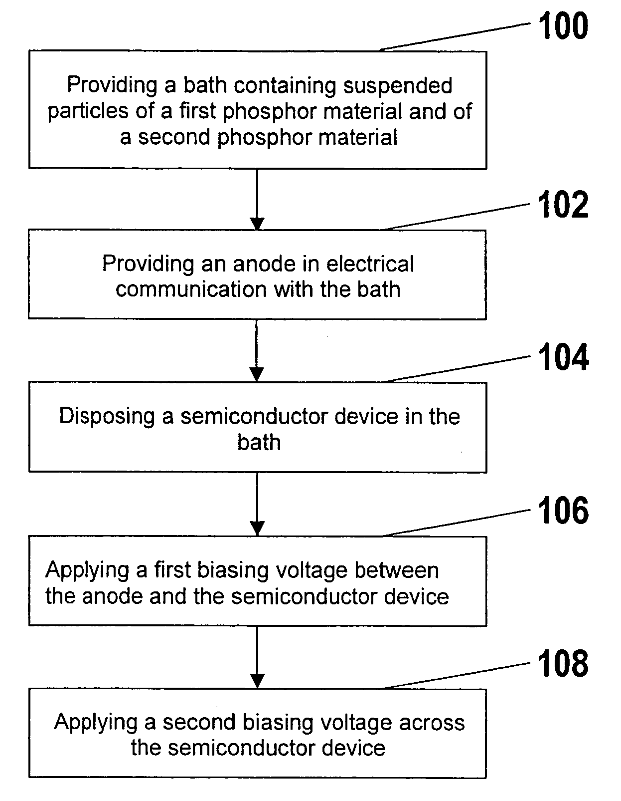
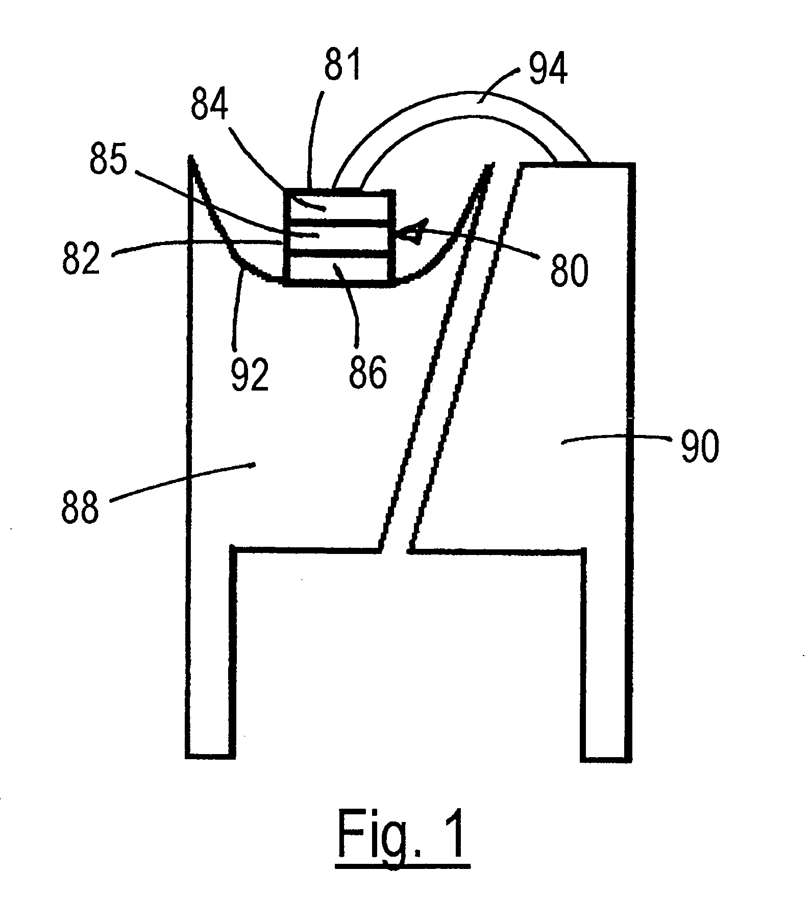
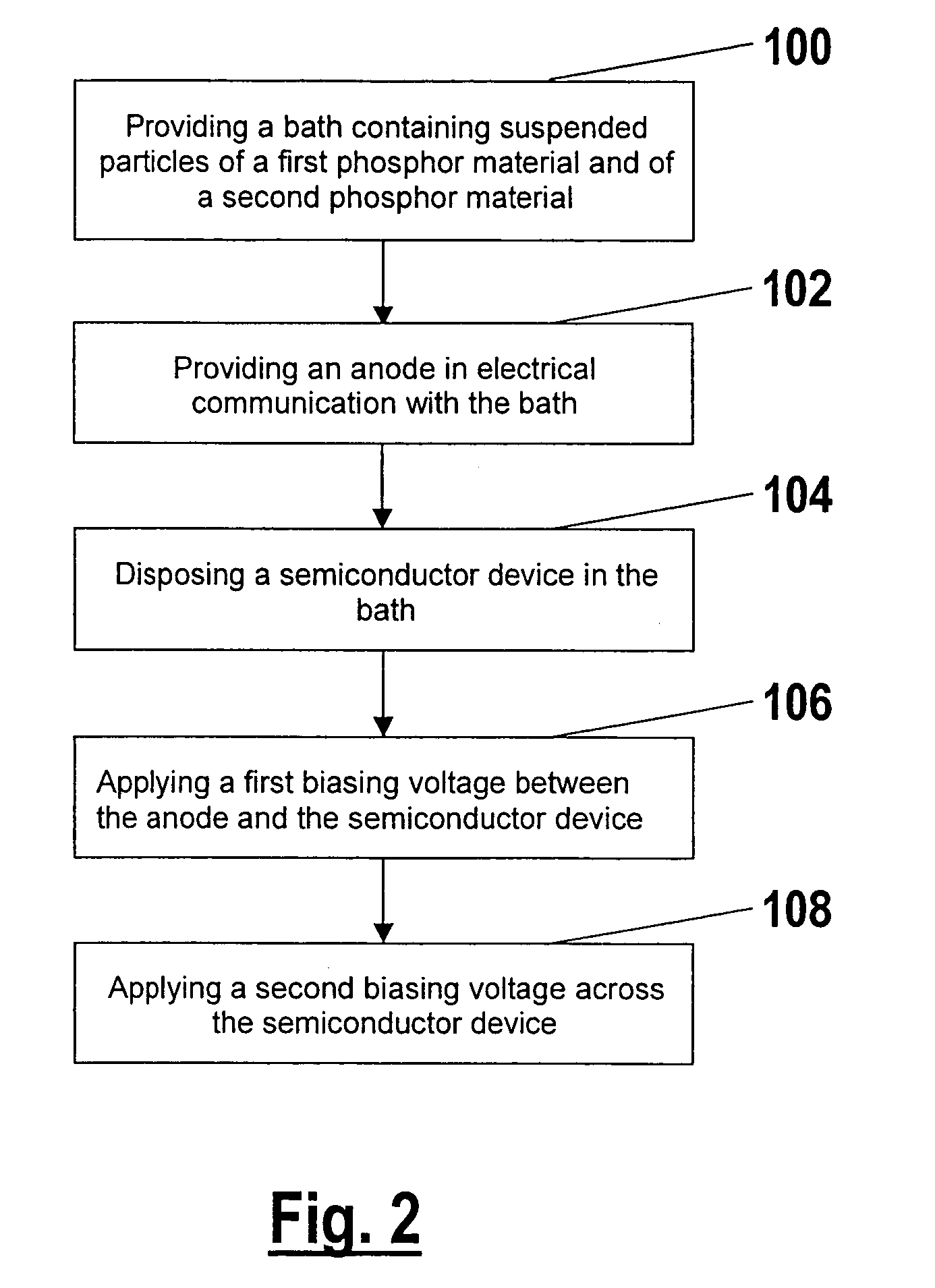
[0023]Before the invention is described in detail, it is to be understood that unless otherwise indicated this invention is not limited to particular materials, reagents, reaction materials, manufacturing processes, or the like, as such may vary. It is also to be understood that the terminology used herein is for purposes of describing particular embodiments only, and is not intended to be limiting. It is also possible in the present invention that steps may be executed in different sequence where this is logically possible. However, the sequence described below is preferred.

[0024]It must be noted that, as used in the specification and the appended claims, the singular forms “a,”“an” and “the” include plural referents unless the context clearly dictates otherwise. Thus, for example, reference to “a phosphor particle” includes a plurality of phosphor particles. In this specification and in the claims that follow, reference will be made to a number of terms that shall be defined to ha...


PUM

PropertyMeasurementUnit
Lengthaaaaaaaaaa
Lengthaaaaaaaaaa
Lengthaaaaaaaaaa

Abstract

Methods of coating a semiconductor device with phosphor particles are disclosed. In the methods, a bath is provided which contains suspended particles of a first phosphor material and suspended particles of a second phosphor material. The particles of the first phosphor material have a mean particle size in the range from about 1 micron to about 6 microns, and the particles of the second phosphor material have a mean particle size in the range from about 12 microns to about 25 microns, wherein the particle size distribution of the phosphor material in the bath is bimodal. The semiconductor device is disposed in the bath containing the suspended particles, and a first biasing voltage is applied between an anode in electrical contact with the bath and the p side to hold the anode at a positive voltage with respect to the p side. A second biasing voltage is applied between the p side and the n side. In particular embodiments, the method results in a substantially conformal coating of the phosphor particles being deposited on at least one surface of the semiconductor structure.

Description

DESCRIPTION[0001]1. Field of the Invention[0002]The invention relates generally to light emitting devices and more particularly to electrophoretic methods of forming phosphor coatings on semiconductor devices.[0003]2. Background of the Invention[0004]Conventional white light sources include such devices as incandescent and fluorescent lamps. Such devices have several undesirable characteristics, including size, power consumption, limited operating life, among others. Alternative white light sources having improved characteristics are desired.[0005]Semiconductor devices have been investigated as alternative sources of white light with a goal of finding white light sources that are both power efficient and cost efficient. Light emitting diodes (LEDs) are compact and emit light of clear color with high efficiency. Because they are solid-state elements, LEDs have long operating lifetimes, have good initial drive characteristics, exhibit good vibration resistance, and withstand repetitiv...

Claims


Application Information

Patent Timeline
IPC IPC(8): C09K11/08H01L21/44H01L21/02H01L33/00C09K11/66C09K11/56C09K11/77C09K11/80C09K11/62H01L33/50
CPCH01L33/50C25D13/12C25D13/22H01L2933/0041H01L2224/32257H01L2224/32245H01L2224/48091H01L2224/48247H01L2224/73265H01L2224/45144H01L2924/13062H01L2924/00014H01L2924/00H01L2924/00012
Inventor CHUA, JANET BEE YINAHMAD, AZLIDASUMMERS, CHRISTOPHER J.MENKARA, HISHAM
Owner BENCH WALK LIGHTING LLC
Why Eureka
Try Eureka