LDMOS device with isolation guard rings

a technology of isolation guard rings and ldmos, which is applied in the direction of semiconductor devices, semiconductor/solid-state device details, electrical apparatus, etc., can solve the problems of degrading device performance, latching effect, and negative voltage creating leakage current, so as to prevent latching, early breakdown and reliability problems, the effect of leakage curren

Inactive Publication Date: 2005-08-02
TAIWAN SEMICON MFG CO LTD
View PDF9 Cites 79 Cited by
  • Summary
  • Abstract
  • Description
  • Claims
  • Application Information

AI Technical Summary

Benefits of technology

[0007]These and other problems are generally solved or circumvented, and technical advantages are generally achieved, by preferred embodiments of the present invention which provide an LDMOS device and method of manufacture thereof wherein leakage current from the drain to the substrate is prevented by the use of a first and second guard ring disposed proximate and around the drain region of the LDMOS device. The first and second guard rings form an NPN parasitic transistor and provide self-isolation for the drain of the LDMOS device.
[0012]Advantages of embodiments of the present invention include providing a LDMOS device design that is current isolated, wherein leakage current is prevented from flowing from the drain to the substrate by the first and second guard rings, which function as an NPN parasitic transistor that self-isolates the drain side of the LDMOS device. Latch-up, early breakdown and reliability issues are prevented by the use of the first and second guard rings of the present invention in an LDMOS device. The drain may be subjected to both low and high voltages without experiencing leakage current, in accordance with embodiments of the present invention.

Problems solved by technology

A problem with the prior art LDMOS device 100 shown in FIG. 1 is that if the LDMOS device 100 is connected to an inductor load, such as to drive a digital versatile disc (DVD), a transient negative voltage may be fed back at the drain 114 when the power is off.
The transient negative voltage can create leakage current.
This leakage IL degrades device performance, causing a latch-up effect, early breakdown, and reliability issues for the LDMOS device 100, as examples.

Method used


Image

  • LDMOS device with isolation guard rings
  • LDMOS device with isolation guard rings
  • LDMOS device with isolation guard rings

Examples


Embodiment Construction

[0021]The making and using of the presently preferred embodiments are discussed in detail below. It should be appreciated, however, that the present invention provides many applicable inventive concepts that can be embodied in a wide variety of specific contexts. The specific embodiments discussed are merely illustrative of specific ways to make and use the invention, and do not limit the scope of the invention.

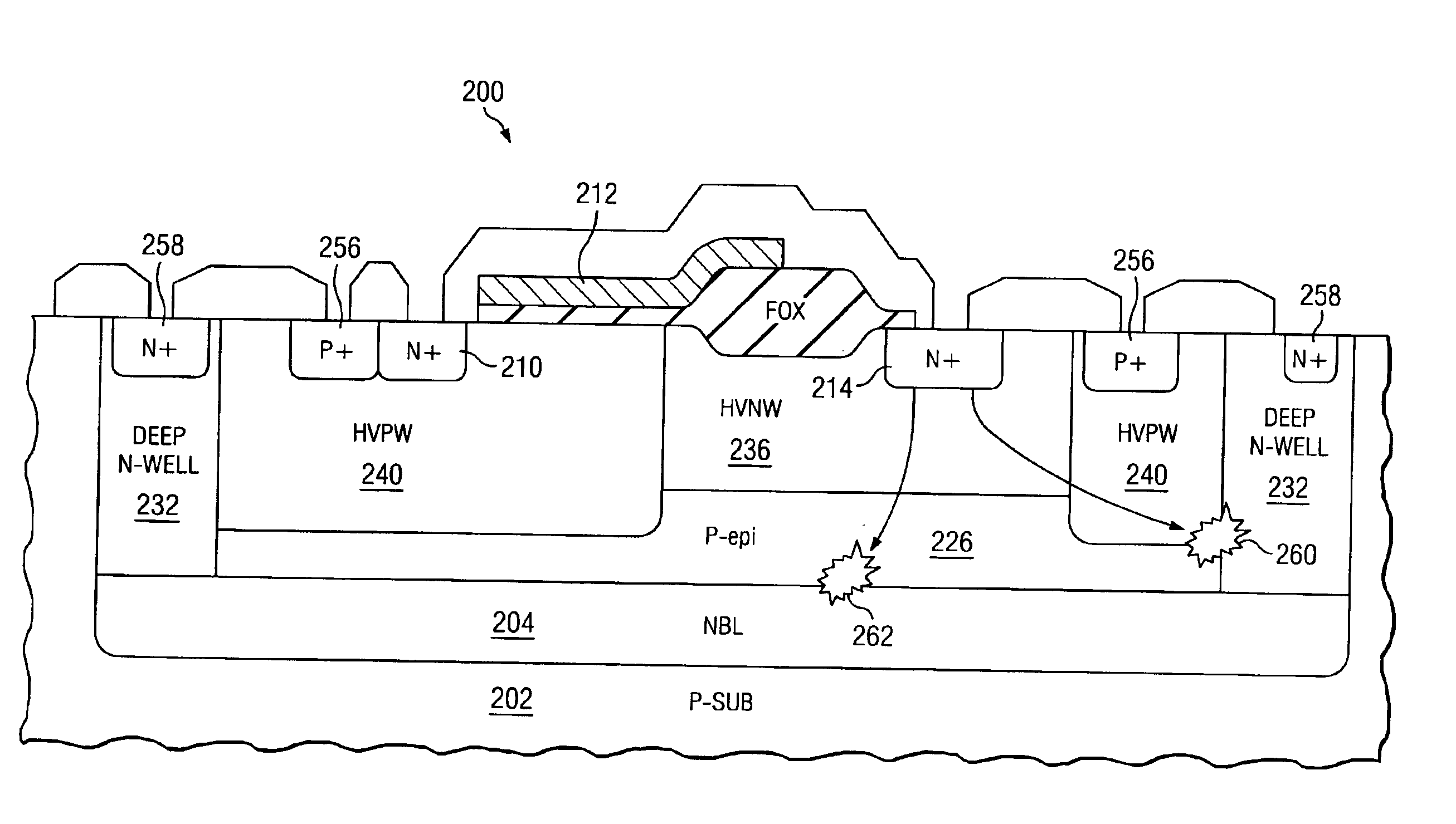
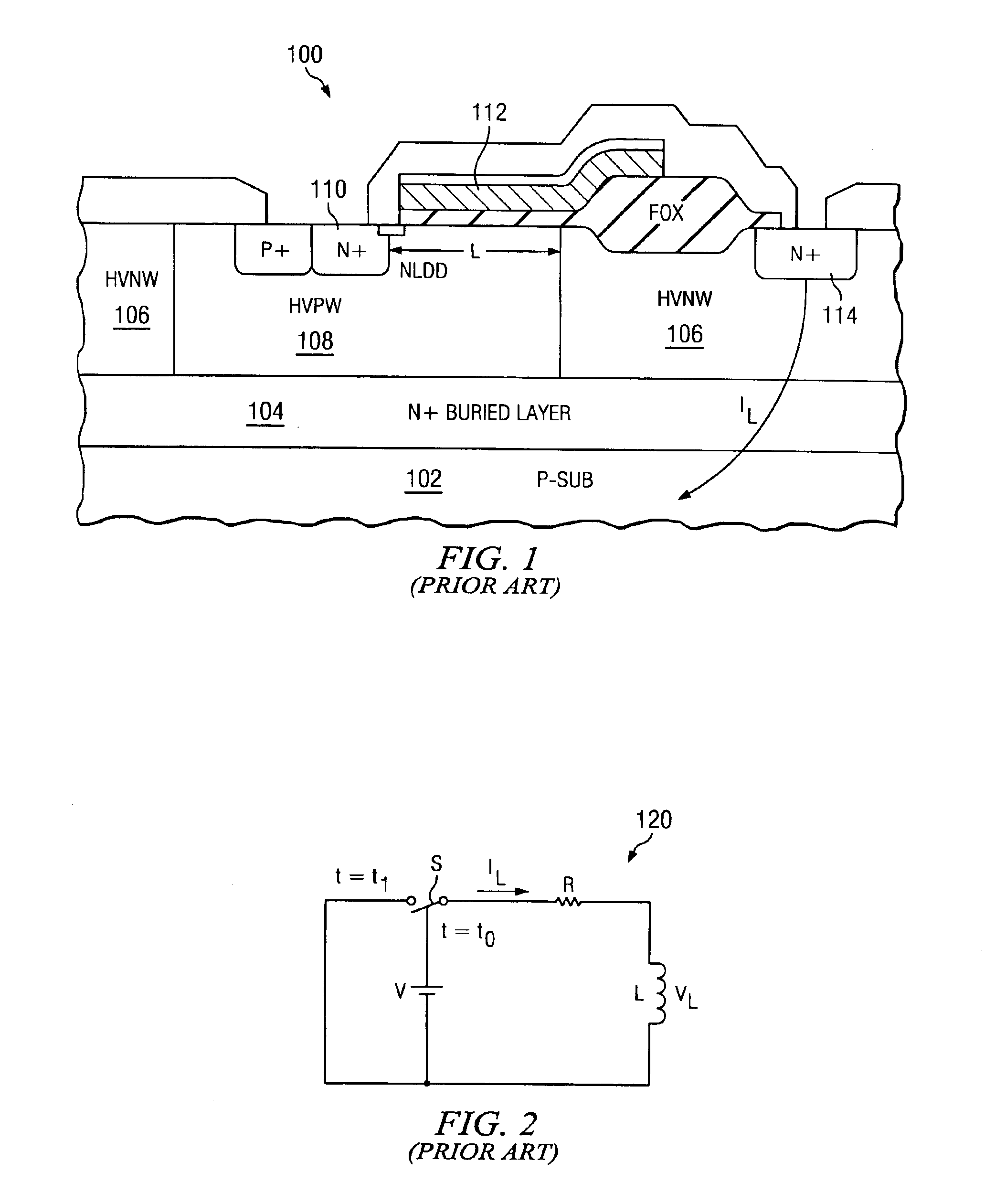
[0022]The present invention will be described with respect to preferred embodiments in a specific context, namely an LDNMOS device, wherein an extended polysilicon gate is used on an extended drain field oxide to reduce surface electric fields (RESURF) and increase breakdown voltage. Embodiments of the invention may also be applied, however, to other LDMOS devices and structures. Although only one LDNMOS device is shown in each figure, there may be many LDNMOS devices formed in each step of the manufacturing process.

[0023]With reference to FIG. 4, therein is shown a cross-sec...


PUM


Abstract

A method of forming a LDMOS semiconductor device and structure for same. A preferred embodiment comprises forming a first guard ring around and proximate the drain of a LDMOS device, and forming a second guard ring around the first guard ring. The first guard ring comprises a P+ base guard ring, and the second guard ring comprises an N+ collector guard ring formed in a deep N-well, in one embodiment. The first guard ring and second guard ring prevent leakage current from flowing from the drain of the LDMOS device to the substrate.

Description

TECHNICAL FIELD[0001]The present invention relates generally to semiconductor devices, and more particularly to a lateral double-diffused metal oxide semiconductor (LDMOS) device and method of manufacture thereof.BACKGROUND[0002]An LDMOS device is basically a metal oxide semiconductor field effect transistor (MOSFET) fabricated using a double-diffusion process with coplanar drain and source regions. A prior art LDMOS device 100 is shown in a cross-sectional view in FIG. 1. An N+ buried layer 104 of silicon is formed within the top portion of a P-substrate 102. A high voltage P well (HVPW) 108 extends downwardly from the top surface of the substrate 102. The HVPW 108 includes an N+ source 110 having a distance L from the junction between an adjacent high voltage N well (HVNW) 106 and the N+ source 110, wherein distance L defines the channel of the device 100. A gate 112 is formed proximate the source 110 over a field oxide (FOX). The LDMOS device 100 includes a drain 114 comprising a...

Claims


Application Information

Patent Timeline
Patent Type & Authority Patents(United States)
IPC IPC(8): H01L29/76H01L29/66H01L31/062H01L31/06H01L21/336H01L27/105H01L29/10H01L29/78
CPCH01L29/1083H01L29/1087H01L29/66659H01L29/7835
Inventor CHEN, FU-HSINLIU, RUEY-HSIN
Owner TAIWAN SEMICON MFG CO LTD
Why Eureka
Try Eureka