

Output buffer circuit and control method therefor
- Summary
- Abstract
- Description
- Claims
- Application Information
AI Technical Summary
Benefits of technology
Problems solved by technology
Method used
Image

Examples
first embodiment
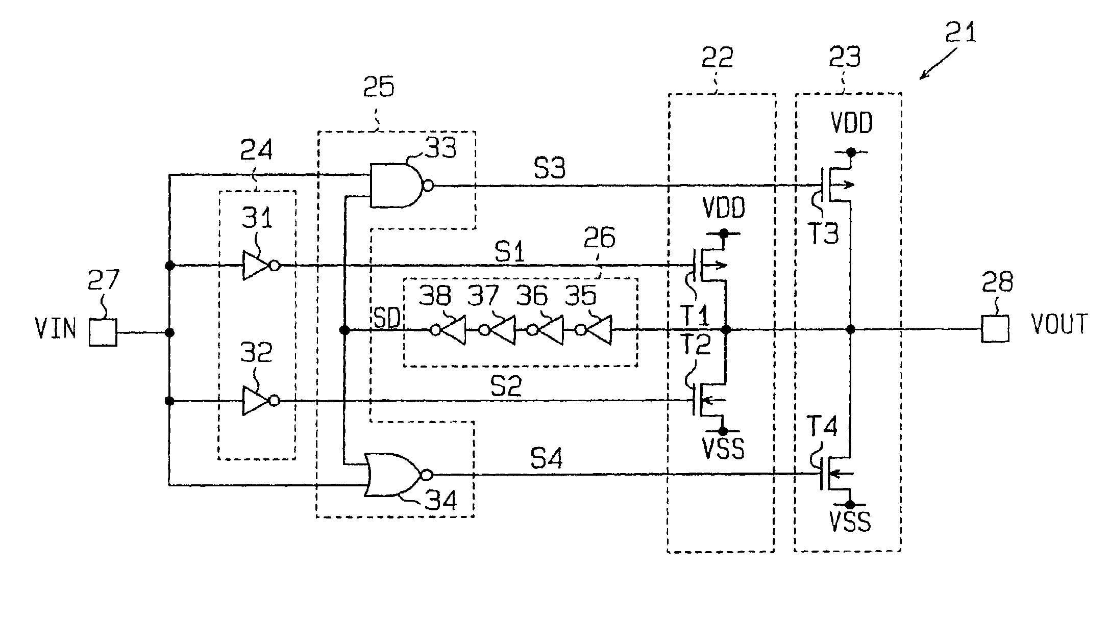
[0047]FIG. 5 is a schematic circuit diagram of an output buffer circuit 21 according to the present invention. The output buffer circuit 21 has first and second drive circuits 22 and 23, first and second control circuits 24 and 25, and a delay circuit 26. The output buffer circuit 21 receives an external input signal VIN from an input terminal 27 and generates an external output signal VOUT which has gentle rising and falling edges corresponding to a predetermined specification. The output buffer circuit 21 outputs the external output signal VOUT from an output terminal 28. The output buffer circuit 21 has a low impedance characteristic with respect to the output terminal 28.
[0048]The first drive circuit 22 generates the external output signal VOUT that has gentle rising and falling edges corresponding to a predetermined specification, and the second drive circuit 23 is provided for the low impedance characteristic.
[0049]The first drive circuit 22 includes a PMOS transistor (first o...
second embodiment
[0073]FIG. 8 is a schematic circuit diagram of an output buffer circuit 41 according to the present invention. The output buffer circuit 41 alters the output impedance value. The output buffer circuit 41 includes first and second drive circuits 22 and 42, first and second control circuits 24 and 43, a delay circuit 26 and three inverter circuits 44, 45 and 46. The second drive circuit 42 includes a plurality of (three in this case) sub-drive circuits 42a, 42b and 42c, and the second control circuit 43 includes three associated sub-control circuits 43a, 43b and 43c.
[0074]The sub-drive circuits 42a, 42b and 42c respectively include PMOS transistors (output transistors) T3a to T3c and NMOS transistors (output transistors) T4a to T4c. At least one of the PMOS transistors T3a-T3c has a different impedance from those of the other.
[0075]The sub-control circuits 43a, 43b and 43c respectively include NAND gates 47a to 47c which generate control signals S3a to S3c for controlling the respect...
fourth embodiment
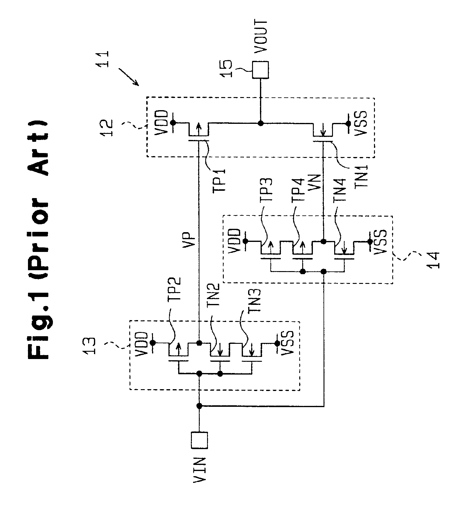
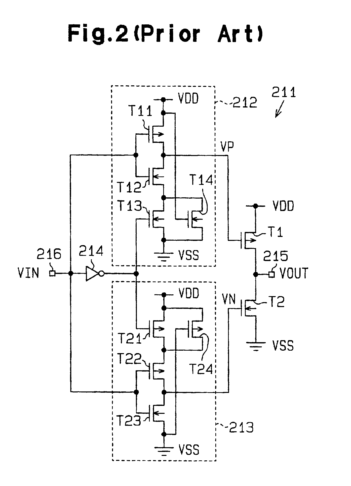
[0082]FIG. 10 is a schematic circuit diagram of a slew-rate control type output buffer circuit 231 according to the present invention. The output buffer circuit 231 has first and second output driving transistors (hereinafter simply called “output transistors”) T1 and T2, first and second slew-rate control circuits (hereinafter simply called “control circuits”) 212 and 213 which perform the ON / OFF control of the respective output transistors T1 and T2 in response to the external input signal VIN, a delay circuit 232 and a signal generator 233.
[0083]The delay circuit 232, which is preferably a buffer circuit, receives the external input signal VIN and generates the delay signal SD which is the external input signal VIN delayed by substantially the same delay time as that of the conventional delay circuit 14.
[0084]The signal generator 233 includes first and second inverter circuits 234 and 235, a NAND gate 236 and a NOR gate 237.
[0085]The first inverter circuit 234 has a low threshold...
PUM
 Abstract
Description
Claims
Application Information