Bitline hard mask spacer flow for memory cell scaling

a memory cell and spacer flow technology, applied in the field of arrayed semiconductor devices, can solve the problems of reduced data storage density, reduced speed and cost, and inability to erase without extra exterior equipment, and achieve the effects of reducing data reliability, and reducing data storage density

Active Publication Date: 2005-08-09
INFINEON TECH LLC
View PDF13 Cites 68 Cited by
  • Summary
  • Abstract
  • Description
  • Claims
  • Application Information

AI Technical Summary

Benefits of technology

[0015]According to one aspect of the invention, the invention is a method of manufacturing a semiconductor device, the method comprising the steps of: forming a charge trapping layer over a substrate; forming a hard mask with openings of a width dimension less than achievable at a resolution limit of lithography; forming buried bitlines in the substrate; and forming a doped region adjacent to at least one of the buried bitlines, wherein the doped region adjacent the at least one of the buried bitlines inhibits a leakage current between the buried bitlines.

Problems solved by technology

EEPROM can be easily erased without extra exterior equipment but with reduced data storage density, lower speed, and higher cost.
Unfortunately, this structure inherently requires a great deal of precision in both programming and reading the differences in the levels to be able to distinguish the bits.
The need in the MLS architecture to precisely control the amount of charge in a memory cell while programming also makes the technology slower and the data less reliable.
It also takes longer to access or “read” precise amounts of charge.
Unfortunately, as the channel size is decreased, there is potential for the semiconductor device to be affected by the short channel effect.
Decreasing the effective channel length can result in an undesirable off-state current passing between the buried bitlines, much like the off-state current in the MOS transistors.
Thus, the undesirable current passing between the buried bitlines limits the further scaling of non-volatile memory devices.
Additionally, in the manufacture of semiconductor devices, there are multiple high temperature cycles (thermal cycles) that may adversely increase off-state leakage current by increasing diffusion of the buried bitlines and reducing the effective channel length.
Further, there is a need to produce such devices by a process which decreases the number of manufacturing steps.

Method used


Image

  • Bitline hard mask spacer flow for memory cell scaling
  • Bitline hard mask spacer flow for memory cell scaling
  • Bitline hard mask spacer flow for memory cell scaling

Examples


Embodiment Construction

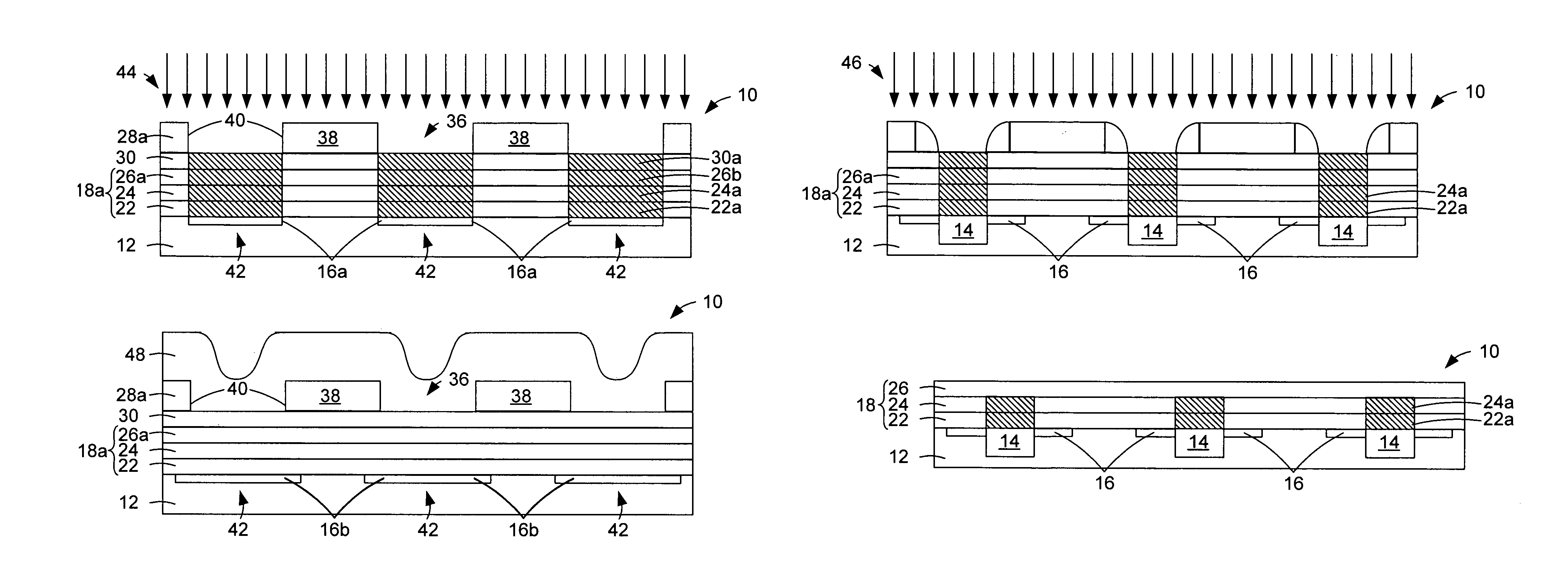
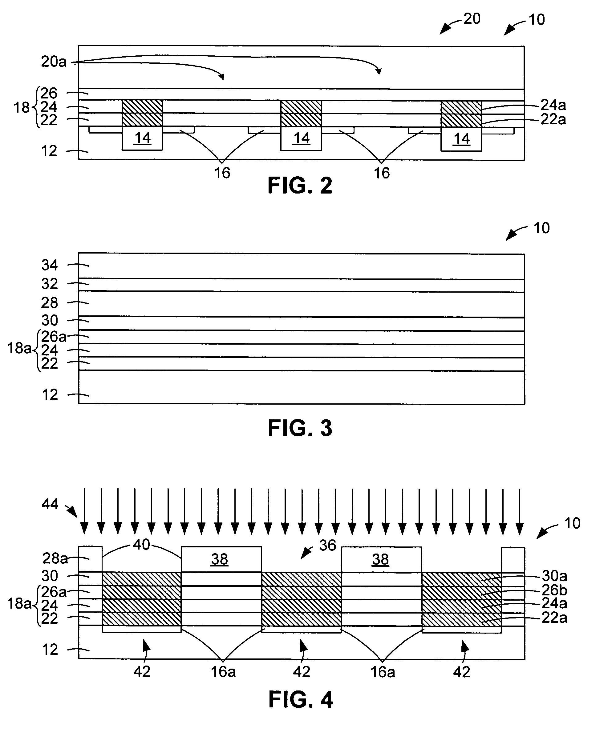
[0025]Referring initially to FIGS. 1 and 2, a structure of the present invention is shown, generally designated as 10. For illustrative purposes, the structure 10 will be described below in relationship to a non-volatile memory device, including a charge trapping non-conducting layer and buried bitlines. The structure 10 may also be referred to herein as the semiconductor device 10. Those having ordinary skill in the art will appreciate that the invention applies to other semiconductor devices that include buried bitlines, e.g., a floating gate FLASH memory device with buried bitlines, as further described below.

[0026]The semiconductor device 10 includes a semiconductor substrate 12 with buried bitlines 14 and doped regions 16 adjacent the buried bitlines 14 formed therein. A dielectric layer 18 is formed over the semiconductor substrate 12. The dielectric layer 18 is interposed between a conductive layer 20 and the semiconductor substrate 12. The conductive layer 20 is patterned so...


PUM


Abstract

The invention is a semiconductor device and a method of forming the semiconductor device. The semiconductor device comprises a substrate; buried bitlines formed in the substrate narrower than achievable at a resolution limit of lithography; a doped region formed adjacent at least one of the buried bitlines; a charge trapping layer disposed over the substrate; and a conductive layer disposed over the charge trapping layer, wherein the doped region adjacent the least one of the buried bitlines inhibits a leakage current between the buried bitlines.

Description

TECHNICAL FIELD[0001]The present invention generally relates to arrayed semiconductor devices. Specifically, the present invention relates to the use of a disposable hard mask with spacers for memory bitline scaling in non-volatile memory devices.BACKGROUND ART[0002]Various types of memories have been developed in the past as electronic memory media for computers and similar systems. Such memories include electrically erasable programmable read only memory (EEPROM) and electrically programmable read only memory (EPROM). Each type of memory had advantages and disadvantages. EEPROM can be easily erased without extra exterior equipment but with reduced data storage density, lower speed, and higher cost. EPROM, in contrast, is less expensive and has greater density but lack erasability.[0003]A newer type of memory called “Flash” EEPROM, or Flash memory, has become extremely popular because it combines the advantages of the high density and low cost of EPROM with the electrical erasabili...

Claims


Application Information

Patent Timeline
Patent Type & Authority Patents(United States)
IPC IPC(8): H01L21/70H01L21/027H01L21/761H01L21/02H01L21/8246H01L27/115
CPCH01L27/115H01L27/11568H10B43/30H10B69/00
Inventor YANG, JEAN Y.RAMSBEY, MARK T.PARK, JAEYONGKAMAL, TAZRIENLINGUNIS, EMMANUIL H.
Owner INFINEON TECH LLC
Why Eureka
Try Eureka