Method and apparatus for forming pattern on thin substrate or the like

a thin substrate and pattern technology, applied in the direction of photomechanical equipment, instruments, printing, etc., can solve the problems of deteriorating throughput, increasing the manufacturing cost of the exposure device, and longer time to be required before the end of the exposur

Inactive Publication Date: 2005-08-09
DAI NIPPON PRINTING CO LTD
View PDF6 Cites 11 Cited by
  • Summary
  • Abstract
  • Description
  • Claims
  • Application Information

AI Technical Summary

Benefits of technology

[0029]A problem to be solved by the present invention is that the mask image is blurred and a desired pattern cannot be formed for the resist, at a position where the image-formed surface and the exposed surface largely separate due to the unevenness in thickness of the glass substrate used for a large-scale liquid crystal display device.

Problems solved by technology

Another problem to be solved is that in a case where the exposure is performed by adding a flattening mechanism, a time to be required before the end of exposure becomes longer and the throughput is deteriorated.
As still another problem, the flattening mechanism is a large-scale device and the manufacturing costs of the exposure device are further increased.

Method used


Image

  • Method and apparatus for forming pattern on thin substrate or the like
  • Method and apparatus for forming pattern on thin substrate or the like
  • Method and apparatus for forming pattern on thin substrate or the like

Examples


Embodiment Construction

[0062]Embodiments of the present invention will be described below with reference to the attached drawings.

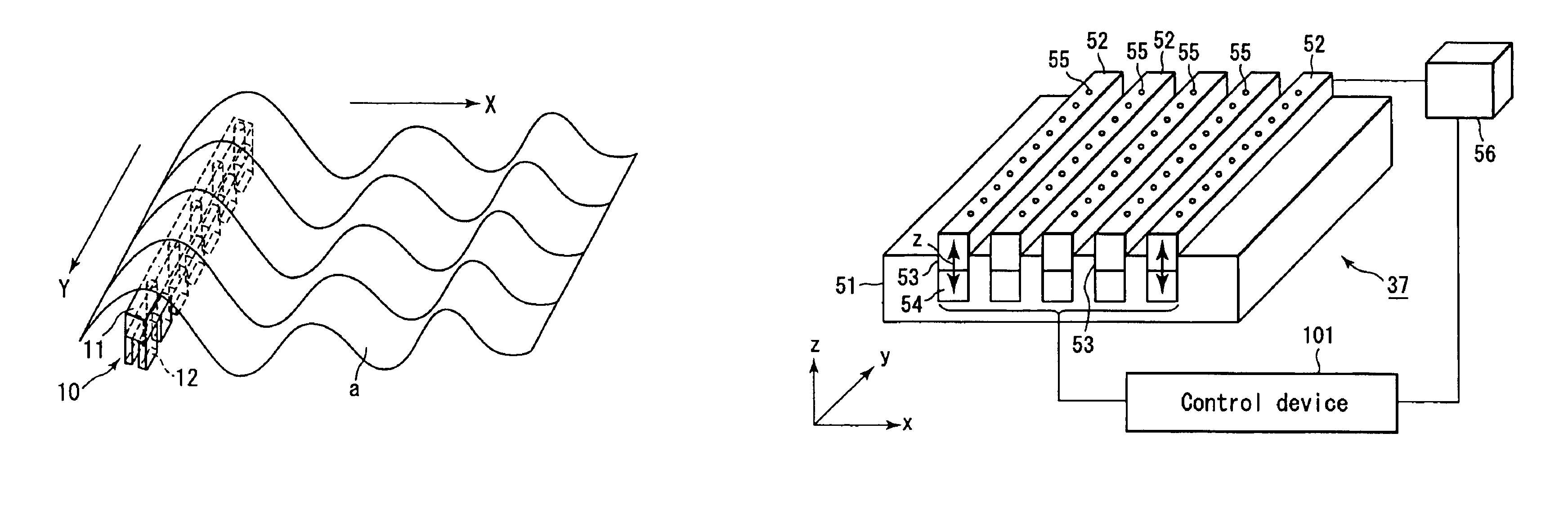
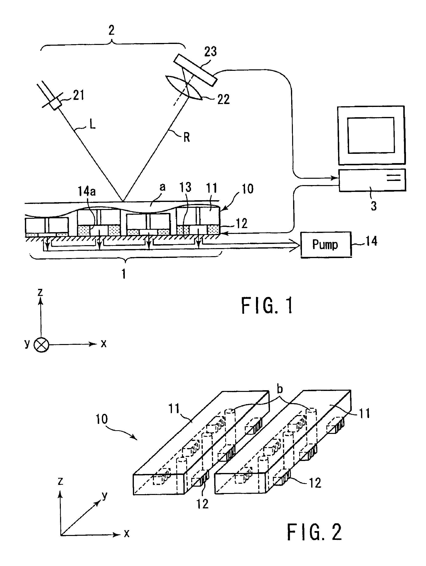
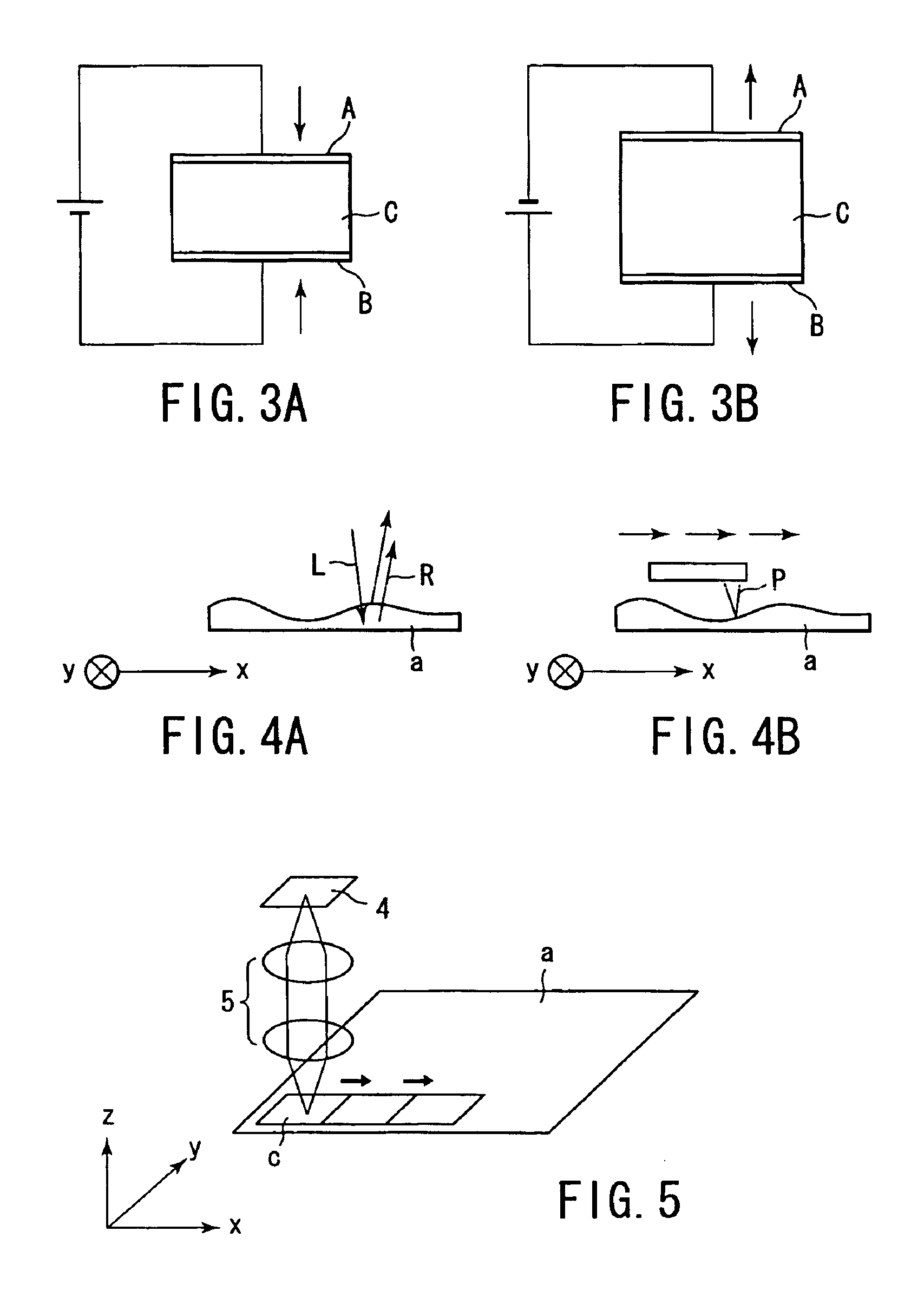
[0063]FIG. 1 is a view for explanation of a structure of a device correcting undulation or thickness unevenness of an influence on an exposed surface, according to an embodiment of the present invention.

[0064]An undulation or thickness unevenness correcting device which corrects undulation and thickness unevenness on a predetermined region i.e., a surface to be exposed, of an object a or a plate-like member such as a glass substrate or a silicon wafer, includes a retaining means (substrate deforming mechanism) 1 which retains a substrate a, an undulation or thickness unevenness correcting means 2 which senses the undulation or thickness unevenness of the substrate a placed on the retaining means 1, and a control device 3 which controls operations of the correcting means 2. For example, a personal computer or the like is available as the control device 3.

[0065]The retaining mean...


PUM

PropertyMeasurementUnit
sizeaaaaaaaaaa
sizeaaaaaaaaaa
sizeaaaaaaaaaa

Abstract

A substrate processing apparatus of the present invention has a retaining base which retains a substrate, a device detecting undulation or thickness unevenness, and a control device which operates the detecting device. The substrate is deformed in a range of a field to be processed, by locally displacing the retaining base on the basis of the detected undulation or thickness unevenness of the substrate. Blurring of an image formed on the substrate can be thereby prevented.

Description

CROSS-REFERENCE TO RELATED APPLICATIONS[0001]This application is based upon and claims the benefit of priority from the prior Japanese Patent Application No. 2002-303364, filed Oct. 17, 2002, the entire contents of which are incorporated herein by reference.BACKGROUND OF THE INVENTION[0002]1. Field of the Invention[0003]This invention relates to an exposure device, a processor and an exposing method for a substrate particularly having large unevenness in thickness as represented by a glass substrate used for a liquid crystal display or the like, a method of producing a thin film transistor, and a method of producing a display device.[0004]2. Description of the Related Art[0005]A glass substrate used for a semiconductor substrate, a liquid crystal display or the like is formed by patterning and stacking a plurality of materials such as semiconductor layers, insulation layers and the like. A technique of lithography is employed for the patterning.[0006]According to the lithography, a ...

Claims


Application Information

Patent Timeline
Patent Type & Authority Patents(United States)
IPC IPC(8): G03F7/20H01L21/027
CPCG03F7/70791G03F7/70783H01L21/027
Inventor TANIGUCHI, YUKIOYAMAGUCHI, HIROTAKATSUJIKAWA, SUSUMU
Owner DAI NIPPON PRINTING CO LTD
Why Eureka
Try Eureka