Hybrid silicon wafer and method of producing the same

a technology of hybrid silicon and silicon wafer, which is applied in the field of hybrid silicon wafer, can solve the problems of increasing the cost of lsi process, and high cost of single crystal wafer having a diameter of 400 mm or more, so as to improve the production yield, reduce production costs, and facilitate the preparation of large ingots

Active Publication Date: 2014-02-11
JX NIPPON MINING & METALS CORP
View PDF19 Cites 4 Cited by
  • Summary
  • Abstract
  • Description
  • Claims
  • Application Information

AI Technical Summary

Benefits of technology

[0020]Thus, the present invention inexpensively provides a so-called hybrid wafer combining polycrystalline silicon and single-crystal silicon by using a general-purpose 300 mm single-crystal and which can be applied to a dummy wafer of 400 mm or more, as well as improves the production yield by improving the strength of the dummy wafer. Consequently, the present invention is able to provide a hybrid silicon wafer comprising the functions of both a polycrystalline silicon wafer and a single-crystal silicon wafer.
[0021]Although a sintered silicon may be used at the polycrystalline silicon portion of the hybrid wafer, since there is a large amount of gas components such as C and O compared to a melted Si ingot and SiC and SiO2 of high hardness precipitate at the crystal grain boundary, the polishing rate is slow in the mirror polishing process compared to the single-crystal silicon portion, and there is a problem in that unevenness will occur in the thickness of the single-crystal silicon portion and the polycrystalline silicon portion. Thus, an object of this invention is to provide a hybrid silicon wafer capable of overcoming the foregoing problems, and provide it more inexpensively.
[0027]As a result of the above, it is possible to provide a hybrid silicon wafer comprising the functions of both a polycrystalline silicon wafer and a single-crystal wafer. Thus, the present invention yields a significant effect of simultaneously possessing the characteristics and function as a single-crystal wafer. Moreover, the bonding stability of the boundary of the polycrystalline portion and the single-crystal portion of the hybrid silicon wafer can be further improved by integrating the hybrid silicon wafer from a molten state.
[0029]In addition, since polycrystalline silicon can be formed by melting silicon around a single-crystal ingot, a large ingot can be prepared easily. Moreover, since the boundary faces are mutually integrated, a hybrid silicon wafer can be manufactured by slicing the prepared complex.
[0030]As described above, the hybrid silicon wafer comprising the functions of both a polycrystalline silicon wafer and a single-crystal wafer is able to considerably improve the production yield and reduce production costs compared to an independent single-crystal wafer of the same size. In addition, the present invention yields a significant effect of being able to prepare an inexpensive dummy silicon wafer of 400 mm or more by using polycrystalline silicon blocks for commercialized solar batteries and waste materials, and a 300 mm single-crystal silicon ingot.
[0031]Furthermore, a dummy silicon wafer prepared by using a polycrystalline silicon ingot having a purity of 6N or higher is characterized in that it will not contaminate the process unit or other components even when it is introduced into the process unit. Moreover, since the polycrystalline silicon is melted and bonded around the single-crystal with a cleavage surface, a significant effect is yielded in that the strength of the wafer can be increased, and the deterioration in the production yield caused by cracks in the cleavage of the wafer can be prevented.

Problems solved by technology

Nevertheless, a single-crystal wafer having a diameter of 400 mm or more is extremely expensive, and consequently its dummy wafer is also expensive, and costs of the LSI process will thereby increase.
Moreover, with a single-crystal silicon wafer of a large diameter; for instance, a diameter of 400 mm or more, there is concern that the cracks of the single-crystal cleavage surface will increase and the production yield will deteriorate compared to a conventional 300 mm wafer.
Although a sintered silicon may be used at the polycrystalline silicon portion of the hybrid wafer, since there is a large amount of gas components such as C and O compared to a melted Si ingot and SiC and SiO2 of high hardness precipitate at the crystal grain boundary, the polishing rate is slow in the mirror polishing process compared to the single-crystal silicon portion, and there is a problem in that unevenness will occur in the thickness of the single-crystal silicon portion and the polycrystalline silicon portion.

Method used


Image

  • Hybrid silicon wafer and method of producing the same
  • Hybrid silicon wafer and method of producing the same

Examples


example 1

[0059]Amorphous silicon (having a purity of roughly 7N excluding dopants and gas components) having an average size of 30 mm to become the raw material of the polycrystalline silicon was placed in a quartz crucible surrounded with carbon, and the temperature was raised to 1500° C. in a vacuum based on high frequency induction heating to melt the silicon.

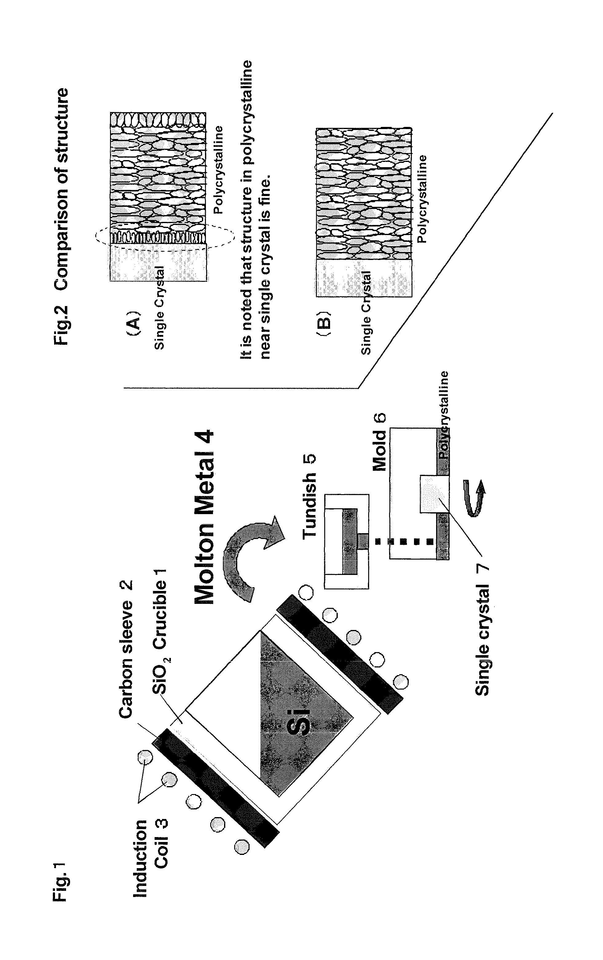
[0060]Meanwhile, as shown in FIG. 1, a single-crystal ingot 7 having a diameter of 200 mm, height of 220 mm and purity of 11N was set in a mold 6 having an inner diameter of 360 mm. The single-crystal ingot 7 was fixed upon setting its plane orientation to a prescribed position and placing a high melting point metal with greater specific gravity than Si thereon so as not move when molten metal is poured by. The overall mold was preheated to 1200° C. in order to reduce the thermal shock.

[0061]Subsequently, the silicon as the molten metal 4 in the crucible was cast up to a height of 100 mm via the tundish 5 while controlling the pour s...

example 2

[0065]Single-crystal silicon waste material having a diameter of roughly 10 mm and purity of 6N to become the raw material of the polycrystalline silicon was placed in a quartz crucible surrounded with carbon, and the temperature was raised to 1520° C. in a vacuum based on high frequency induction heating to melt the silicon.

[0066]Meanwhile, as shown in FIG. 1, a single-crystal ingot 7 having a diameter of 300 mm and height of 150 mm was set in a mold 6 having an inner diameter of 500 mm. The single-crystal ingot 7 was fixed upon setting its plane orientation to a prescribed position and so that it will not move when molten metal is poured by placing a high melting point metal with greater specific gravity than Si thereon.

[0067]The overall mold was preheated to 1250° C. in order to reduce the thermal shock. Subsequently, the silicon 4 as the molten metal in the crucible 1 was cast up to a height of 80 mm via the tundish 5 while controlling the pour spout, and the single-crystal ingo...


PUM

PropertyMeasurementUnit
average crystal grain sizeaaaaaaaaaa
diameteraaaaaaaaaa

Abstract

Provided is a hybrid silicon wafer in which molten state polycrystalline silicon and solid state single-crystal silicon are mutually integrated, comprising fine crystals having an average crystal grain size of 8 mm or less at a polycrystalline portion within 10 mm from a boundary with a single-crystal portion. Additionally provided is a method of manufacturing a hybrid silicon wafer, wherein a columnar single-crystal silicon ingot is sent in a mold in advance, molten silicon is cast around and integrated with the single-crystal ingot to prepare an ingot complex of single-crystal silicon and polycrystalline silicon, and a wafer shape is cut out therefrom. The provided hybrid silicon wafer comprises the functions of both a polycrystalline silicon wafer and a single-crystal wafer.

Description

BACKGROUND OF THE INVENTION[0001]1. Field of the Invention[0002]The present invention relates to a hybrid silicon wafer comprising the functions of both a polycrystalline silicon wafer and a single-crystal wafer, and to the method of manufacturing such a hybrid silicon wafer.[0003]2. Description of the Related Art[0004]In the silicon semiconductor manufacturing process, a wafer prepared based on single-crystal growth is primarily used. This single-crystal silicon wafer has increased in size with the times, and it is anticipated that the inner diameter will become φ400 mm or larger in the near future. In addition, a so-called mechanical wafer for testing is now required in order to establish the apparatus and peripheral technology necessary for the semiconductor manufacturing process.[0005]Generally speaking, since this kind of mechanical wafer is subject to fairly high precision testing, it needs to possess characteristics that are similar to the mechanical physicality of single-cry...

Claims


Application Information

Patent Timeline
Patent Type & Authority Patents(United States)
IPC IPC(8): C01B33/02B29D7/00B32B3/02B32B9/04B32B13/04
CPCC30B33/06C30B29/06C30B11/00C01B31/02C01B32/05Y10T428/21
Inventor TAKAMURA, HIROSHISUZUKI, RYO
Owner JX NIPPON MINING & METALS CORP
Why Eureka
Try Eureka