Fault tolerant scan chain for a parallel processing system

a parallel processing system and scan chain technology, applied in the field of parallel processing systems, can solve the problems of affecting system performance, affecting system speed, increasing system noise, etc., and achieve the effect of high-grade fault toleran

Inactive Publication Date: 2005-08-09
NORMAN RICHARD S
View PDF5 Cites 40 Cited by
  • Summary
  • Abstract
  • Description
  • Claims
  • Application Information

AI Technical Summary

Benefits of technology

[0027]Thus the present invention provides a highly robust fault tolerant scan chain suitable for scanning (and/or controlling a configuration of) a parallel processing system. The scan chain implements parallel redundant scan chains that follow physically diverse paths through the parallel processing system. For each IC under test, a set of redundant TAPs perform a boundary scan, and the test results are combined by voting. The TAPs of each set are physically diverse, in tha...

Problems solved by technology

Well known disadvantages of the use of such a modular design approach include the comparatively large physical distances separating each IC of the system (which adversely affects system speed), and increased system noise due, among other things, to Radio Frequency Interference (RFI) and impedance mismatches between “on-chip” circuit traces and the PC board lines between the IC packages.
All of these factors negatively impact system performance.
However, a primary limiting factor in integrated circuit fabrication is that, as the size of an IC increases, so does the probability that manufacturing defects (e.g., a dust particle on the surface of the IC or physical defects in the IC) will damage at least part of the circuitry on the wafer.
This problem is typically expressed in terms of “yield”; that is, the number of serviceable IC's that can be manufactured from each wafer.
As the size of an IC increases toward the total wafer area, the expected yield drops to close to zero, thereby effectively prohibiting the development of practical systems covering the entire surface of the wafer.
Common sources of defects include dust particles on a wafer surface during manufacture.
However, this is not always the case; some faults are not related to defects, and some defects do not produce faults.
Both of these techniques imply a h...

Method used


Image

  • Fault tolerant scan chain for a parallel processing system
  • Fault tolerant scan chain for a parallel processing system
  • Fault tolerant scan chain for a parallel processing system

Examples


Embodiment Construction

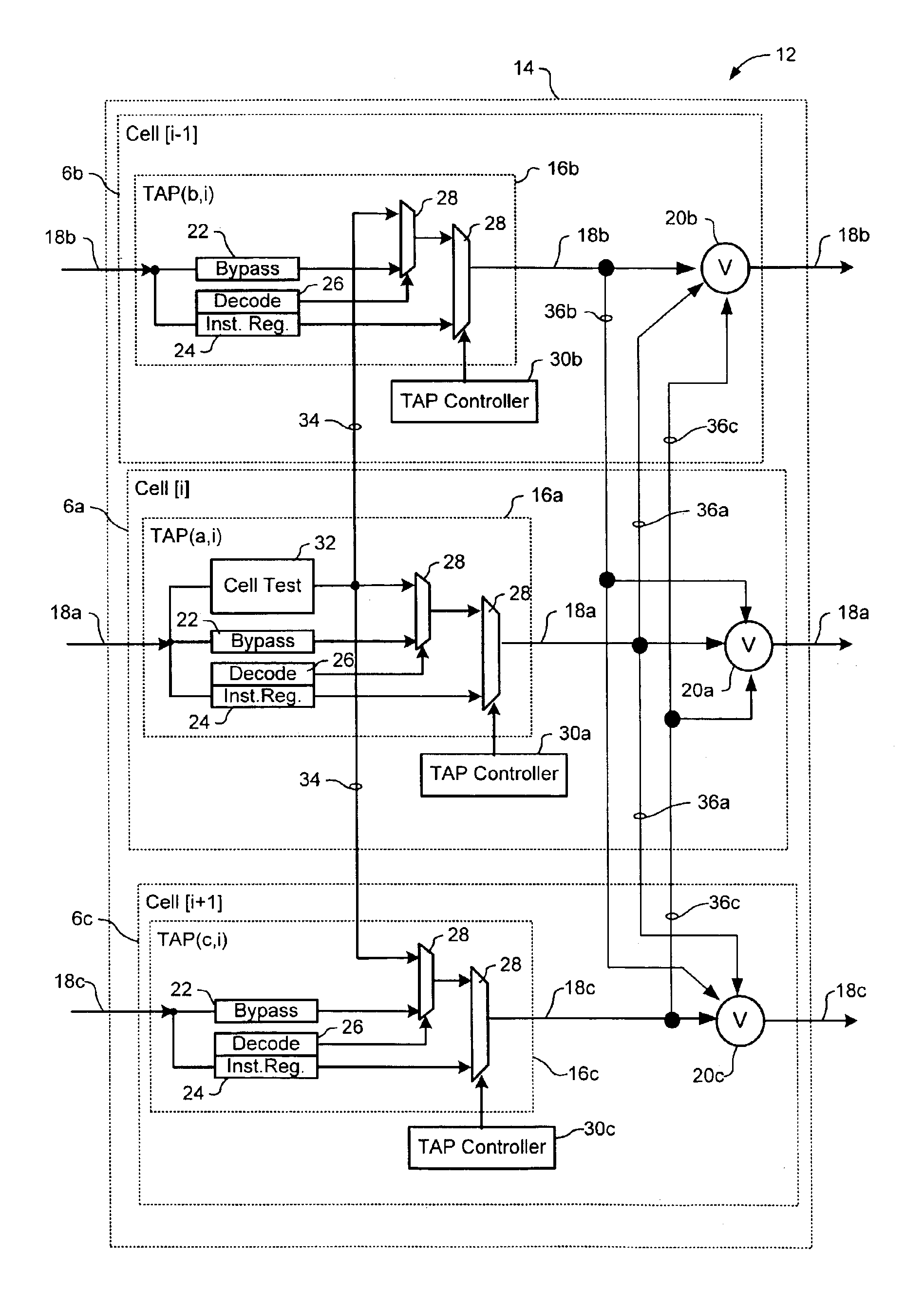
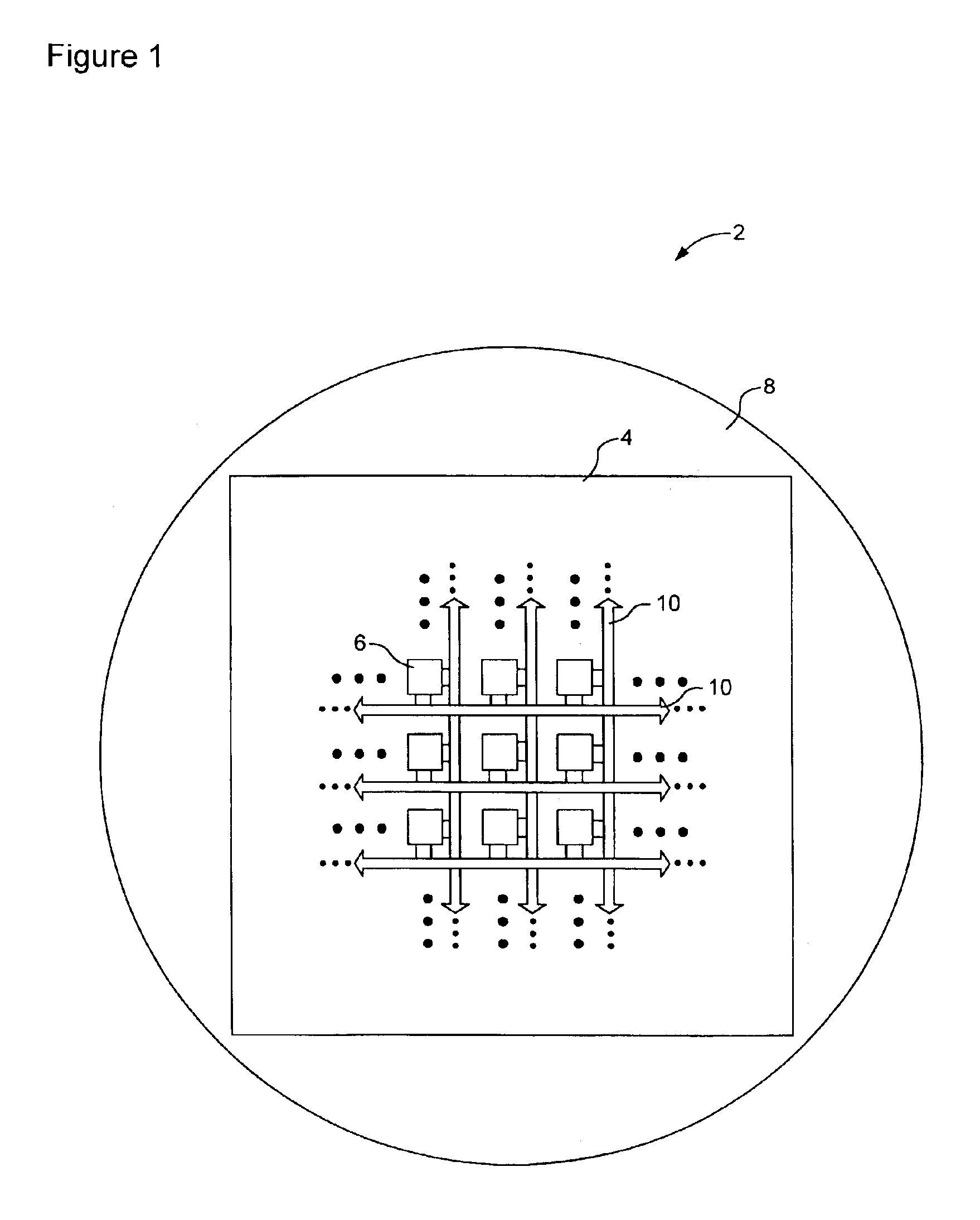
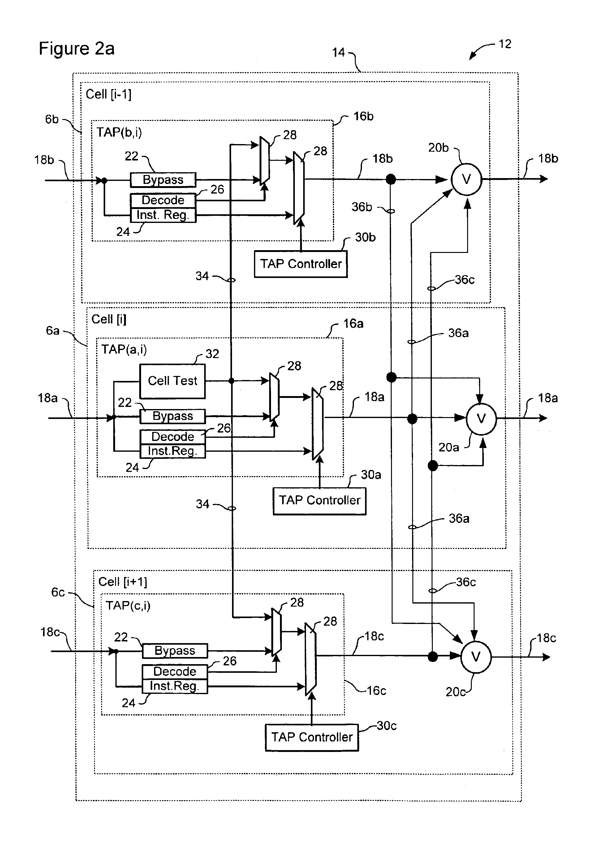
[0034]The present invention provides a fault tolerant scan chain for a wafer-scale parallel processing system. FIG. 1 schematically illustrates principle features of an exemplary wafer-scale parallel processing system in which the present invention may be deployed.

[0035]As shown in FIG. 1, the wafer-scale parallel processing system 2 generally comprises a rectangular (other shapes are possible) matrix 4 of substantially identical cells 6 disposed on a wafer 8 (or, more broadly, a substrate 8). A mesh of communications busses 10 link the cells 6 and carry data signals between cells 6 within the matrix 4, and between the matrix 4 and external devices (not shown). Each communications bus 10 is associated with a respective set (i.e., a row or a column) of cells 6, and includes a plurality of parallel channels (not shown), which may be configured to carry serial or parallel data signals. Each communications bus 10 includes a respective access point for each one of its associated cells 6,...


PUM


Abstract

A highly robust fault tolerant scan chain is designed for scanning (and/or controlling a configuration of) a parallel processing system. The scan chain implements parallel redundant scan chains that follow physically diverse paths through the parallel processing system. For each IC under test, a set of redundant TAPs perform a boundary scan, and the test results are combined by voting. The TAPs of each set are physically diverse, in that they are physically located in separate power domains of the parallel processing system. As a result, the scan chain is robust to faults affecting power and/or control signal supply to any one power domain. Respective input and output dummy cells at opposite extreme ends of the scan chain provide a graceful separation and recombination of the redundant parallel scan chains, and so renders the architecture of the scan chain transparent to external boundary scan circuit elements.

Description

CROSS-REFERENCE TO RELATED APPLICATIONS[0001]This is the first application filed for the present invention.[0002]This application claims priority to U.S. Provisional Patent Application No. 60 / 341,238, filed Dec. 20, 2001 which are incorporated herein by reference.MICROFICHE APPENDIX[0003]Not Applicable.TECHNICAL FIELD[0004]The present invention relates to parallel processing systems, and in particular to a fault tolerant scan chain for a parallel processing system.BACKGROUND OF THE INVENTION[0005]Complex electronic systems are typically designed using multiple integrated circuit (IC) packages mounted on a printed circuit board with interconnects between the packages provided by traces on the printed circuit board. This approach to system design is highly versatile, because a designer can develop a wide range of different systems by selecting from a comparatively limited number of standard IC packages having well defined functionality. Isolation and correction of defects is also simp...

Claims


Application Information

Patent Timeline
IPC IPC(8): G01R31/3185G01R31/28
CPCG01R31/318536
Inventor SAVARIA, YVONLU, MENG
Owner NORMAN RICHARD S
Why Eureka
Try Eureka