Organic electric-field light-emitting element

a technology of electric field and light-emitting element, which is applied in the direction of discharge tube luminescnet screen, other domestic articles, natural mineral layered products, etc., can solve the problems of reducing the luminous efficiency of the injected electrons from the cathode and relatively reducing the injected electrons

Inactive Publication Date: 2005-08-16
IDEMITSU KOSAN CO LTD
View PDF17 Cites 37 Cited by
  • Summary
  • Abstract
  • Description
  • Claims
  • Application Information

AI Technical Summary

Benefits of technology

[0009]According to a third aspect of the present invention, an organic EL element is provided which comprises an anode layer, an organic luminescent layer, a cathode layer and an electron injecting layer between the organic luminescent layer and the cathode layer. The electron injecting layer comprises a hydro

Problems solved by technology

However, in the organic EL elements disclosed by H2(1990)-139893 and H2(1990)-196475, the mobility of electrons injected from

Method used


Image

  • Organic electric-field light-emitting element
  • Organic electric-field light-emitting element
  • Organic electric-field light-emitting element

Examples


first embodiment

[First Embodiment]

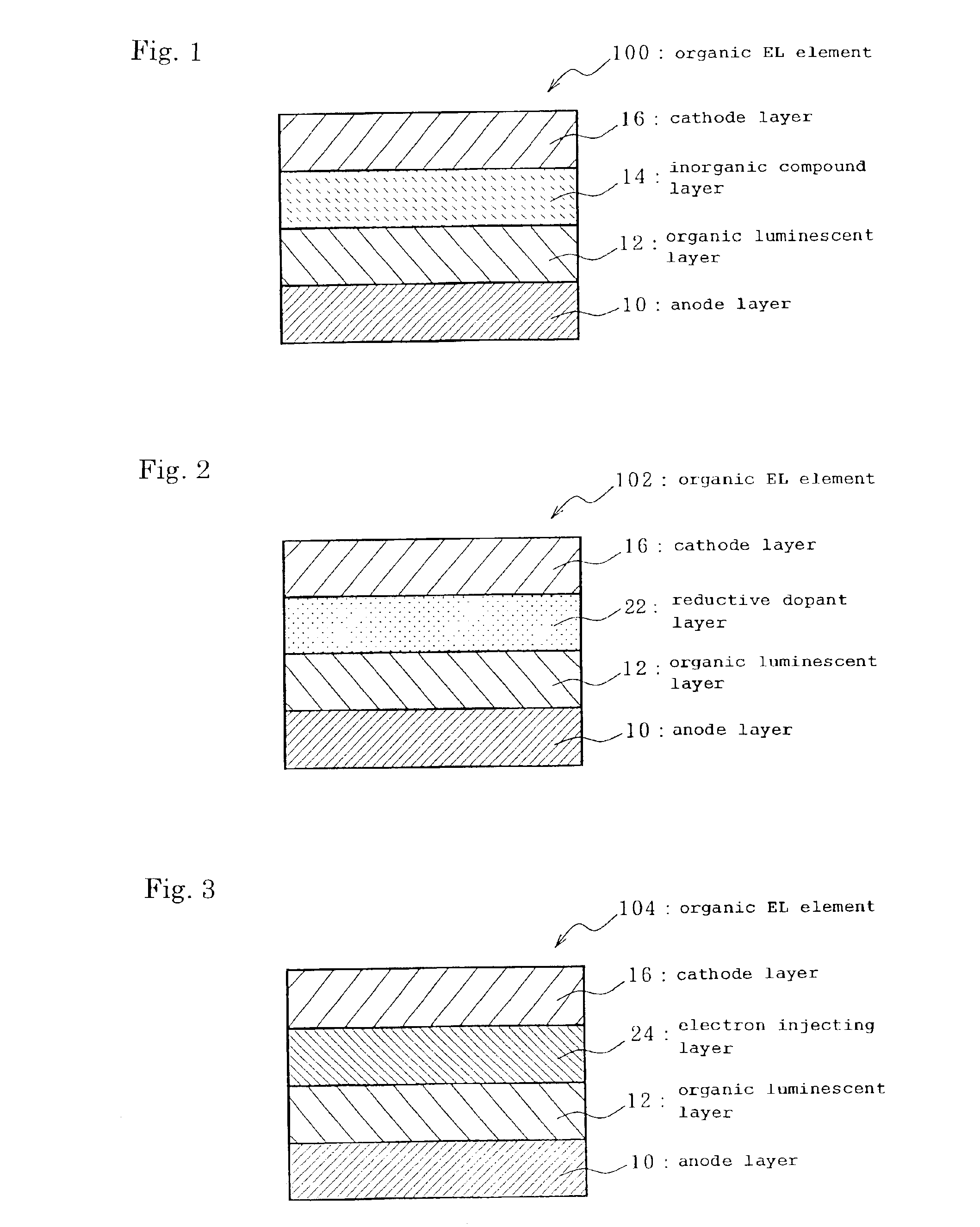
[0016]A first embodiment of the organic EL element according to the present invention will be described with reference to FIG. 1. FIG. 1 is a sectional view of an organic EL element 100, showing the structure of an anode layer 10, an organic luminescent layer 12, an inorganic compound layer 14 and a cathode layer 16 laminated on a substrate (not shown) in this order.

[0017]Here, the organic luminescent layer 12 and inorganic compound layer 14 will be mainly described since they are features of the first embodiment. The other members such as the anode layer 10 and cathode layer 16 will be briefly described about their structures and manufacturing methods. For the members particularly not described, they can be of structure known in the art and manufactured by methods known in the art.

(1) Organic Luminescent Layer

(i) Materials 1

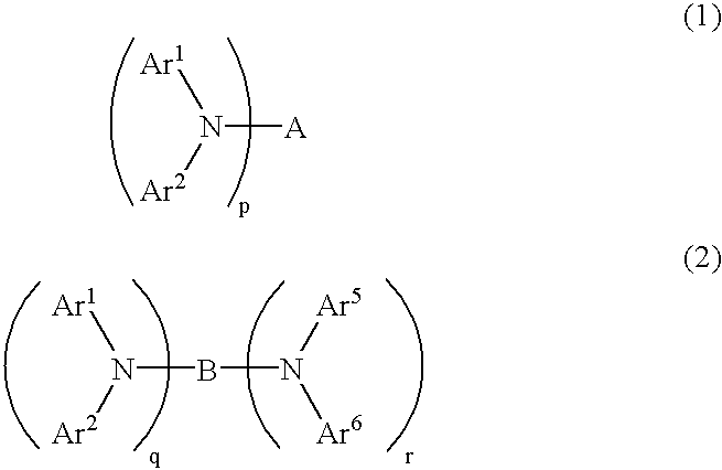
[0018]The above-mentioned aromatic amine compounds of the formulas (1) and (2) are used in an organic luminescent layer. The use of such aroma...

second embodiment

[Second Embodiment]

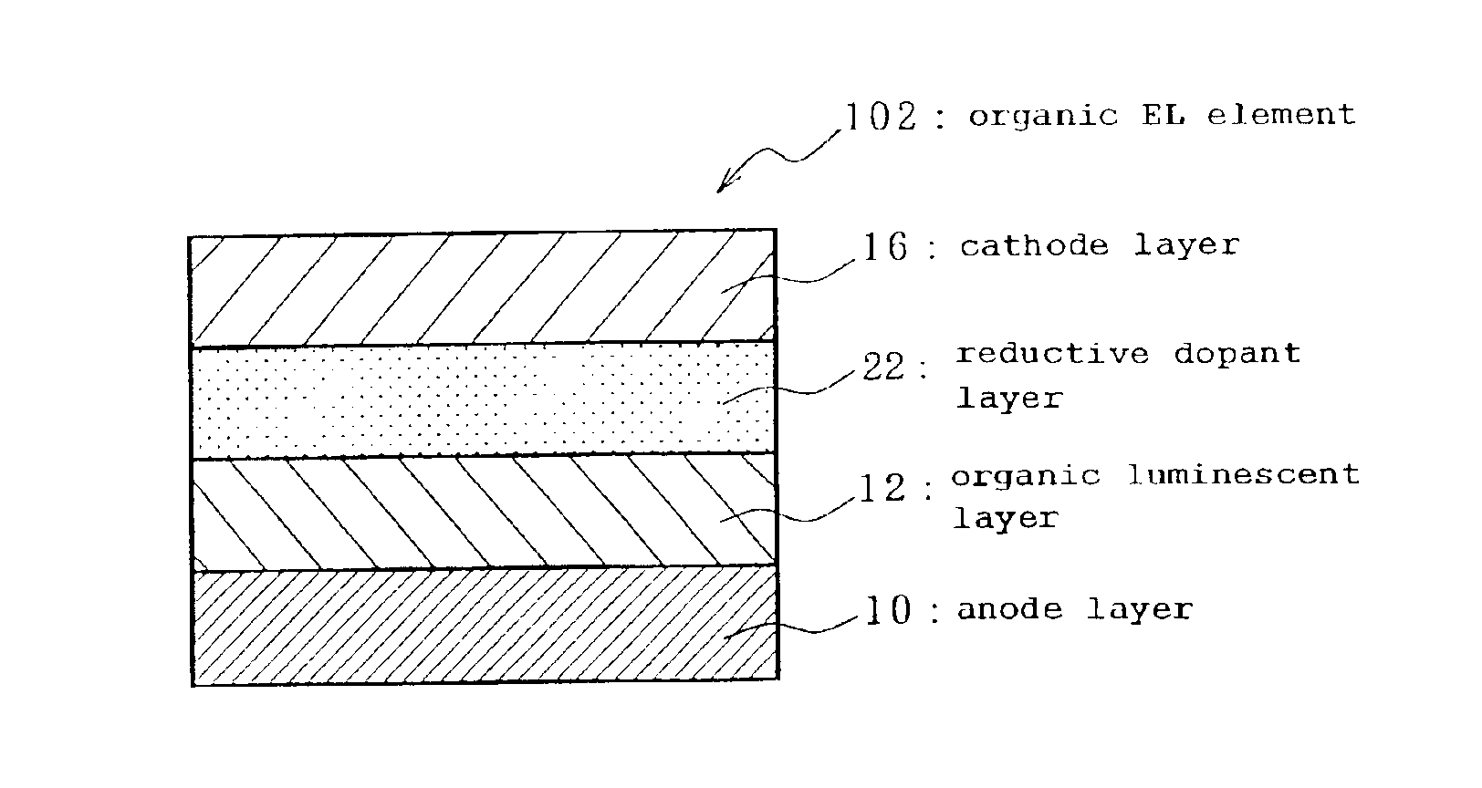
[0068]A second embodiment of the organic EL element according to the present invention will be described with reference to FIG. 2. FIG. 2 is a sectional view of an organic EL element 102, showing the structure of an anode layer 10, an organic luminescent layer 12, a reductive dopant layer 22 and a cathode layer 16 laminated in this order.

[0069]Such reductive dopant layer (hereinafter may referred to as an interface layer) functions to enhance the ability of injecting electrons. Thus, due to the provision of the reductive dopant layer, electrons can be easily injected or transported to the organic luminescent layer, thereby allowing high-speed response of the organic EL element.

[0070]The reductive dopant layer, which is a feature of the second embodiment, will be mainly described. The other members such as the organic luminescent layer can be of structure similar to the first embodiment.

(1) Materials

[0071]Any reductive dopants which have the reductivity to aromatic...

third embodiment

[Third Embodiment]

[0092]A third embodiment of the organic EL element according to the present invention will be described with reference to FIG. 3. FIG. 3 is a sectional view of an organic EL element 104, showing the structure of an anode layer 10, an organic luminescent layer 12, an electron injecting layer 24 and a cathode layer 16 laminated in this order.

[0093]The electron injecting layer comprises a hydrocarbon compound with an anthracene nucleus or a fluoranthene nucleus. The energy gap of the compound is 2.7 eV or more. Further, the organic luminescent layer comprises an aromatic amine compound represented by the formula (3) and / or an aromatic amine compound represented by the formula (4). The aromatic amine compounds of the formulas (3) and (4) are compounds which are represented by the formulas (1) and (2) but may contain a styryl group and an alkenyl group. The above-stated description and examples on the aromatic amine compounds of the formulas (1) and (2) can be applied t...


PUM

PropertyMeasurementUnit
Energyaaaaaaaaaa
Luminanceaaaaaaaaaa
Luminescenceaaaaaaaaaa

Abstract

In an organic electroluminescent element comprising an anode layer, an organic luminescent layer, an inorganic compound layer (or reductive dopant layer) and a cathode layer; the organic luminescent layer comprises an aromatic amine compound of a formula (1), and/or an aromatic amine compound of a formula (2)
wherein A, B, and Ar1 to Ar6 are independently a C6-60 aromatic group which does not contain a styryl group nor an alkenyl group, at least one of A, Ar1, Ar2, or B, Ar3 to Ar6 contains at least three condensed aromatic rings, and p, q and r of a condensation number are an integer of 1 to 6. The element has significantly long half-life and high luminance even at low driving voltages.

Description

TECHNICAL FIELD[0001]The present invention relates to an organic electric-field light-emitting element (hereinafter referred to as an organic electroluminescent (EL) element) and, more particularly to an organic EL element suitably employed in display devices for personal and industrial use, light sources of printer heads and the like.BACKGROUND ART[0002]Japanese Patent Laid-open Nos. H2(1990)-139893, H2(1990)-196475 and H2(1990)-196475 disclose an organic EL element provided with an inorganic semiconductive thin layer and an organic luminescent layer between electrodes for easier injection of electrons and the like. In the organic EL element, an inorganic semiconductive thin layer is formed on an anode, and an organic luminescent layer and a cathode are further formed thereon, which inorganic semiconductive thin layer is made of an inorganic semiconductive material such as carbon, germanium, silicon, tin, silicon carbide, boron nitride, boron phosphide and gallium nitride.[0003]Jap...

Claims


Application Information

Patent Timeline
IPC IPC(8): C09K11/06C09K9/02H01L51/05H01L51/30H05B33/14H05B33/22H01L51/50H01L51/00
CPCC09K11/06H01L51/0052H01L51/0058H01L51/0059H01L51/006H05B33/14H05B33/22C09K2211/1007C09K2211/1011C09K2211/1014H01L51/0054H01L51/0056H01L51/0077H01L51/5012H01L2251/308Y10S428/917H10K85/624H10K85/622H10K85/626H10K85/633H10K85/631H10K85/615H10K85/30H10K50/11H10K2102/103
Inventor ARAKANE, TAKASHIFUKUOKA, KENICHIHOSOKAWA, CHISHIO
Owner IDEMITSU KOSAN CO LTD
Why Eureka
Try Eureka