Early response to plasma/charging damage by special pattern design of active region

a technology of active region and early response, applied in the direction of individual semiconductor device testing, semiconductor/solid-state device testing/measurement, instruments, etc., can solve the problems of high risk of damage to the thin film of the insulation film, the degradation of the reliability of the gate oxide by plasma, and the inability to detect the damage early

Inactive Publication Date: 2005-08-16
TAIWAN SEMICON MFG CO LTD
View PDF8 Cites 4 Cited by
  • Summary
  • Abstract
  • Description
  • Claims
  • Application Information

AI Technical Summary

Benefits of technology

[0013]In accordance with the objects of the invention, a method of early and effective detection of plasma damage to a gate oxide layer by a special design of the active region is achieved. A plasma-damage testing structure is fabricated by providing a gate electrode overlying an active area of a semiconductor substrate wherein a gate oxide layer underlies the gate electrode. A portion of the active area underlying the gate electrode has sharp corners. The plasma-damage testing structure is exposed to a plasma environment. Electrical tests are performed to detect plasma damage to the plasma-damage testing structure. This model provides an accurate evaluation of slight plasma damage to actual MOSFET's.

Problems solved by technology

An insulating film this thin is highly susceptible to damage such as from ion and electron bombardment from plasmas during backend processing.
Plasma-induced degradation of gate oxide reliability is a key issue in achieving high performance MOSFET's.
In addition, both types of structures may be either edge-intensive or area-intensive.
However, it is difficult for these structures to catch plasma-induced damage in a timely manner if the damage is very slight.

Method used


Image

  • Early response to plasma/charging damage by special pattern design of active region
  • Early response to plasma/charging damage by special pattern design of active region
  • Early response to plasma/charging damage by special pattern design of active region

Examples


Embodiment Construction

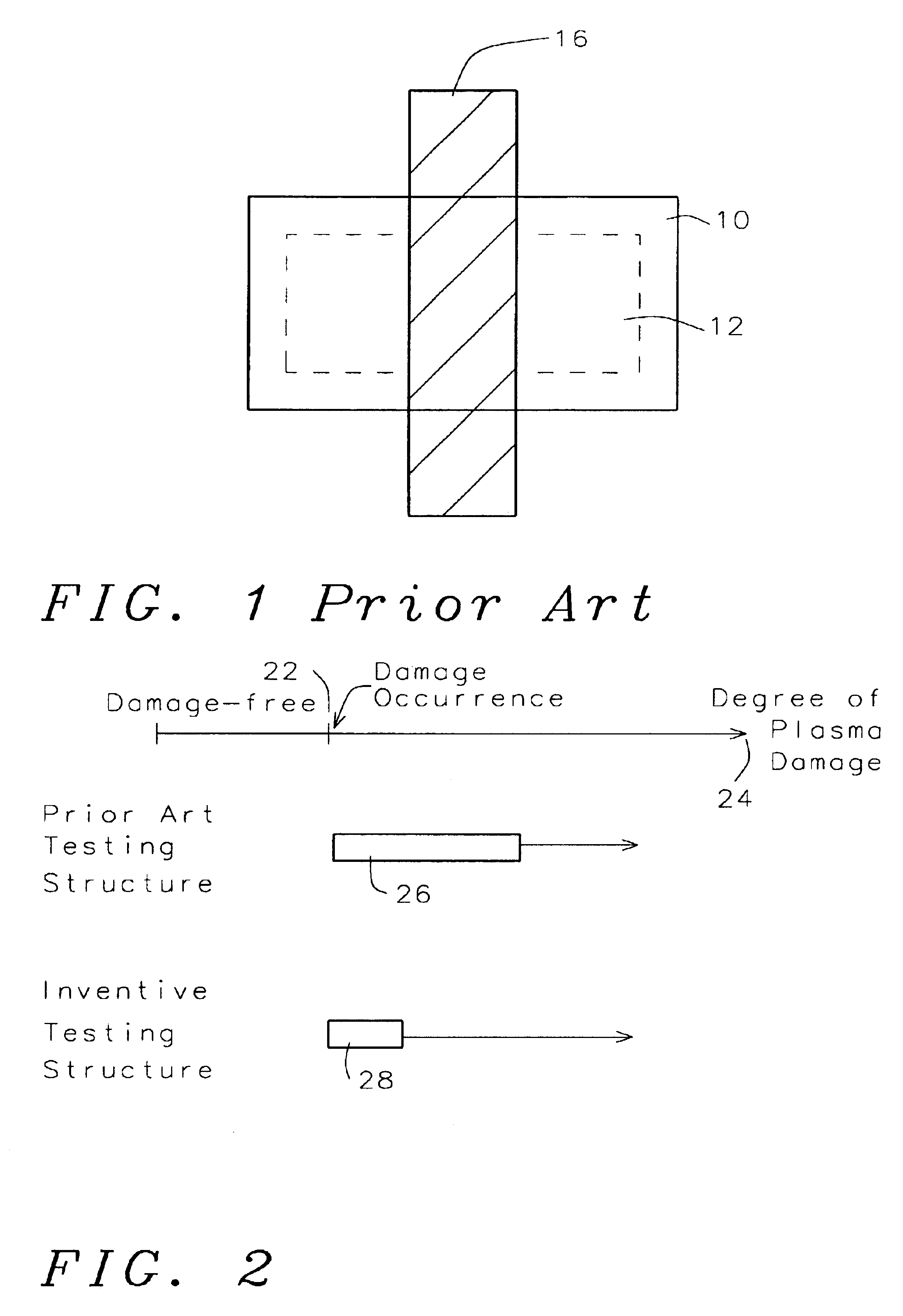
[0022]Referring now to FIG. 1, there is illustrated a conventional plasma-damage testing structure of the prior art. Active area 10 is shown. Field oxide area 12 has been formed over the semiconductor substrate in the active area. Polysilicon gate 16 is shown within the active area. The gate oxide layer, not shown, underlies and is covered by the polysilicon gate 16.

[0023]FIG. 2 illustrates the degree of plasma-induced damage to the gate oxide shown across the top of the figure where no damage occurs to the left of line 22. Increasing damage is shown to the right of line 22 in the direction of the arrow 24. Slight damage occurs immediately to the right of line 22. With a testing structure of the prior art, such as that shown in FIG. 1, there is a large “blind spot”26 where damage occurs, but is not revealed by the testing structure. Greater damage to the right of the blind spot 26 can be caught by the testing structure.

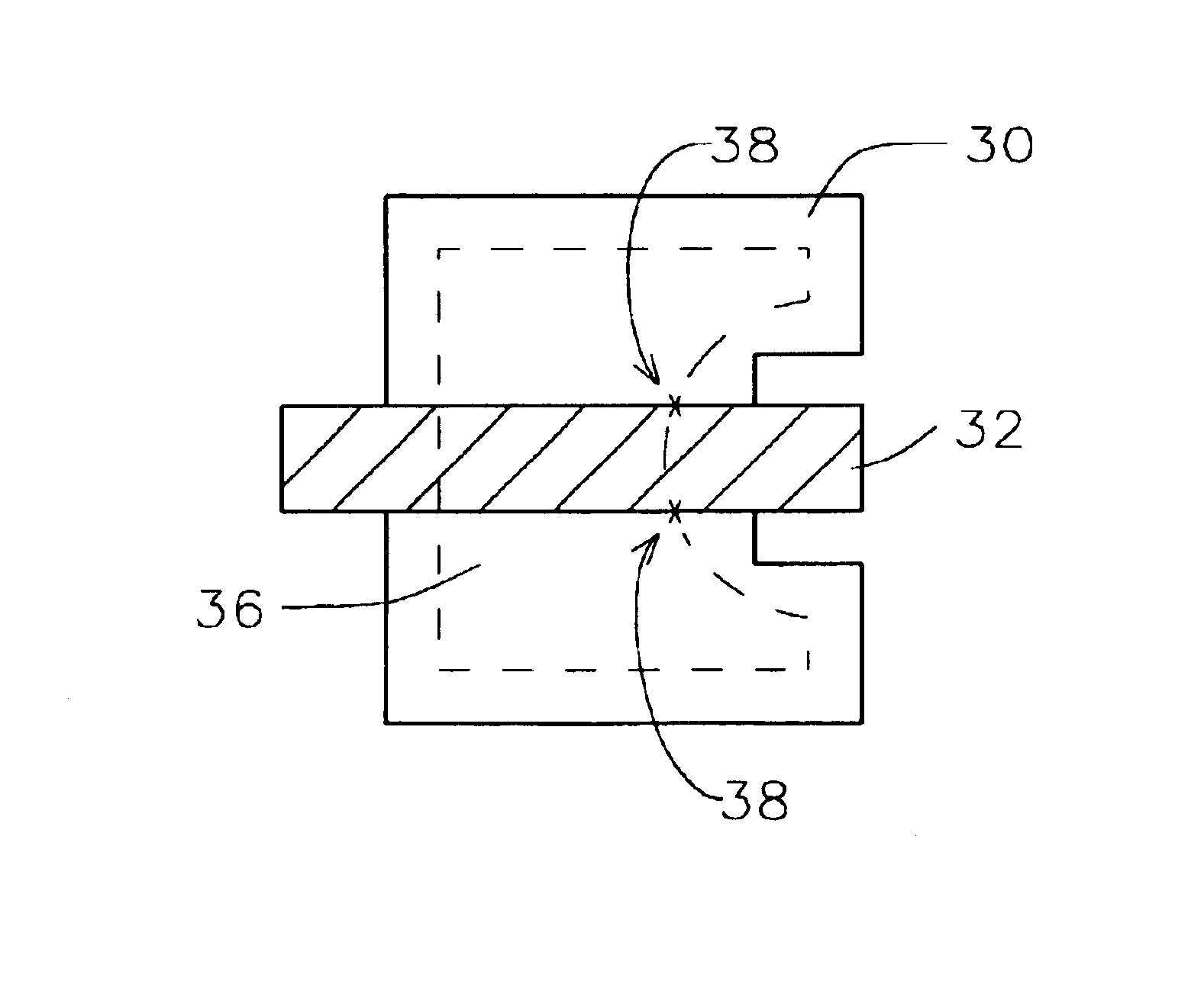
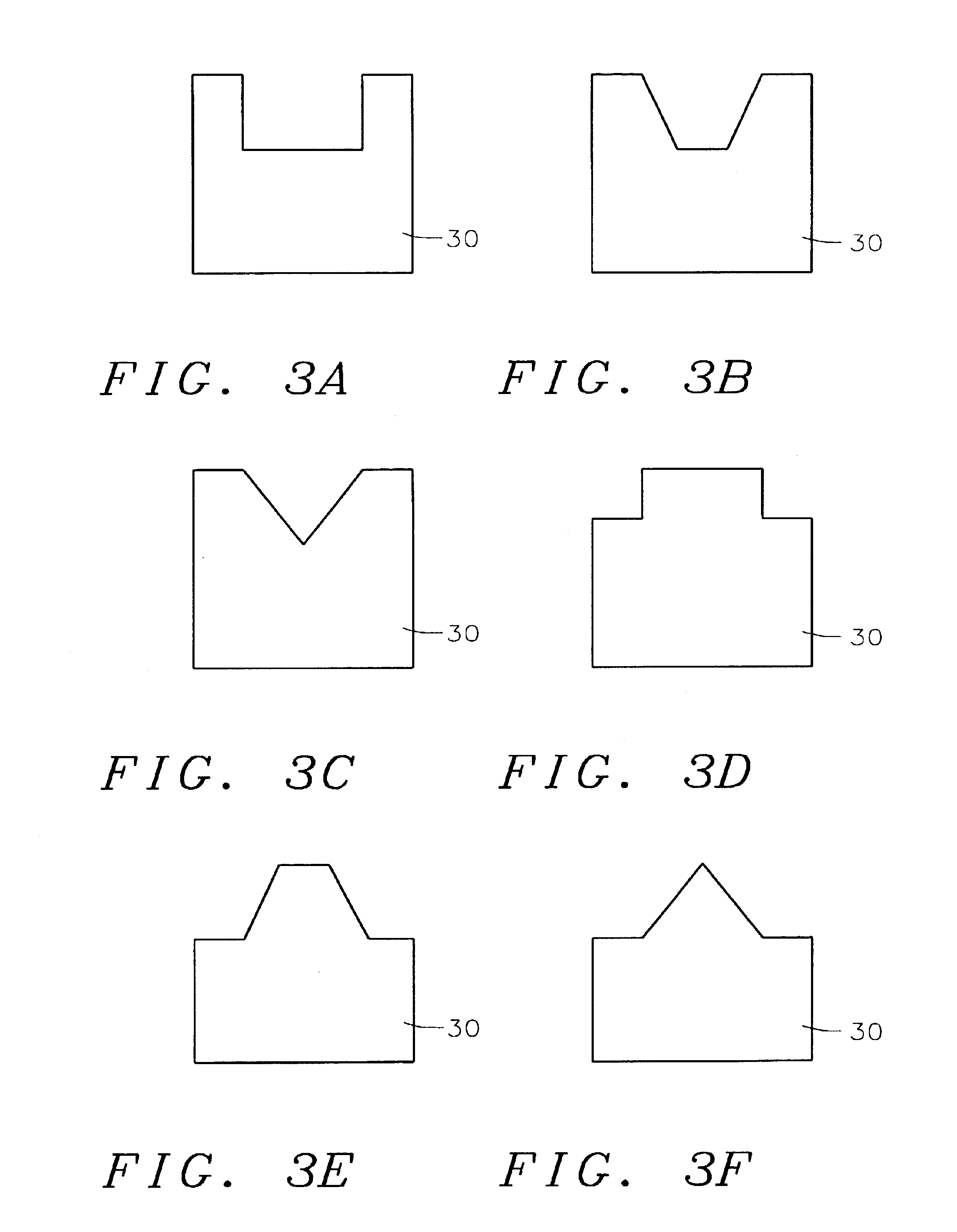
[0024]In contrast, with the testing structure of the present inv...


PUM


Abstract

A method of early and effective detection of plasma damage to a gate oxide layer by a special design of the active region is achieved. A plasma-damage testing structure is fabricated by providing a gate electrode overlying an active area of a semiconductor substrate wherein a gate oxide layer underlies the gate electrode. A portion of the active area underlying the gate electrode has sharp corners. The plasma-damage testing structure is exposed to a plasma environment. Electrical tests are performed to detect plasma damage to the plasma-damage testing structure. This model provides an accurate evaluation of plasma damage to actual MOSFET's.

Description

[0001]This is a division of patent application Ser. No. 09 / 356,002, filing date Jul. 16, 1999 U.S. Pat. No. 6,593,157, Early Response To Plasma / Charging Damage by Special Pattern Design Of Active Region, assigned to the same assignee as the present invention.BACKGROUND OF THE INVENTION[0002](1) Field of the Invention[0003]The present invention relates to the fabrication of integrated circuit devices, and more particularly, to a method of early detection of plasma / charging damage in the fabrication of integrated circuit devices.[0004](2) Description of the Prior Art[0005]The manufacture of large scale integrated circuits involves hundreds of processing steps. Most of these processing steps involve depositing layers of material, patterning them by photolithographic techniques, and etching away the unwanted portions. Plasma etching processes are often used because they are dry processes and they provide the cleanliness and degree of control required in integrated circuit manufacture.[0...

Claims


Application Information

Patent Timeline
Patent Type & Authority Patents(United States)
IPC IPC(8): H01L23/544
CPCH01L22/34H01L2924/0002H01L2924/00
Inventor CHEN, BOR-CHENGTAI, YU-FENG
Owner TAIWAN SEMICON MFG CO LTD
Why Eureka
Try Eureka