Dry etching apparatus, etching method, and method of forming a wiring

a technology of etching apparatus and wiring, applied in the direction of identification means, instruments, transistors, etc., can solve the problems of non-uniformity of substantial electric power applied to the entire surface of a substrate, etching defects, and enhancement of productivity, so as to enhance the uniformity of rectangular substrates in the plan

Inactive Publication Date: 2005-08-16
SEMICON ENERGY LAB CO LTD
View PDF17 Cites 213 Cited by
  • Summary
  • Abstract
  • Description
  • Claims
  • Application Information

AI Technical Summary

Benefits of technology

[0017]Therefore, with the foregoing in mind, it is an object of the present invention to provide a dry etching apparatus capable of treating a large substrate, and an etching method capable of enhancing in-plane uniformity of a rectangular substrate to be treated.

Problems solved by technology

Conventionally, there is a limit to a treatment ability of a dry etching apparatus, which causes problems in terms of enhancement of productivity.
More specifically, in the case of using a rectangular substrate, a substantial electric power applied to the entire surface of a substrate becomes non-uniform, and an electric power density is varied between the central portion of the substrate and the comer portions thereof.
Therefore, in the case of using a conventional etching apparatus, the selection ratio at comer portions of an electrode becomes lowest, causing etching defects.
The etching defects may decrease a yield.
If a substrate is enlarged in the future, this problem is considered to become more conspicuous.

Method used


Image

  • Dry etching apparatus, etching method, and method of forming a wiring
  • Dry etching apparatus, etching method, and method of forming a wiring
  • Dry etching apparatus, etching method, and method of forming a wiring

Examples


embodiment mode 1

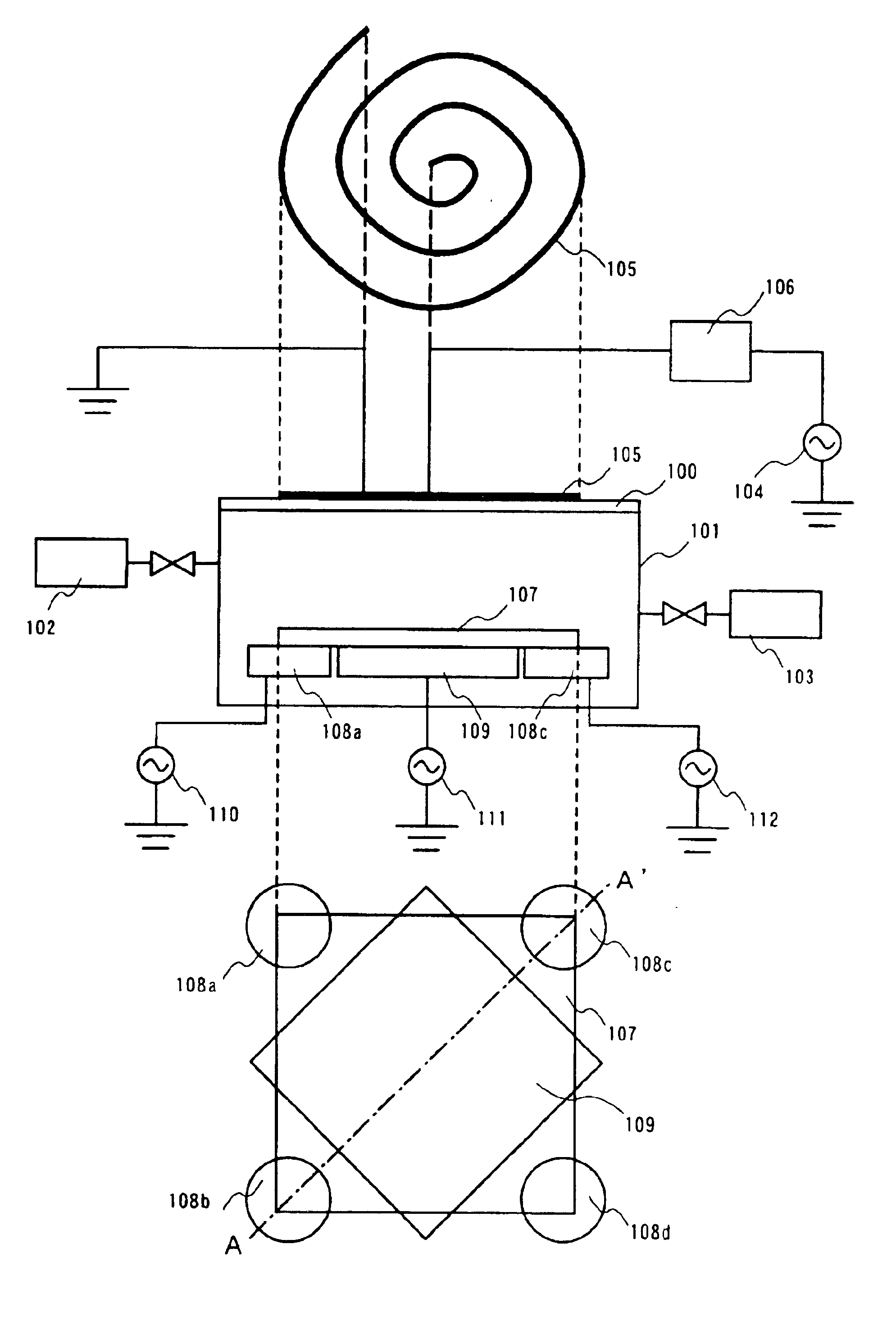
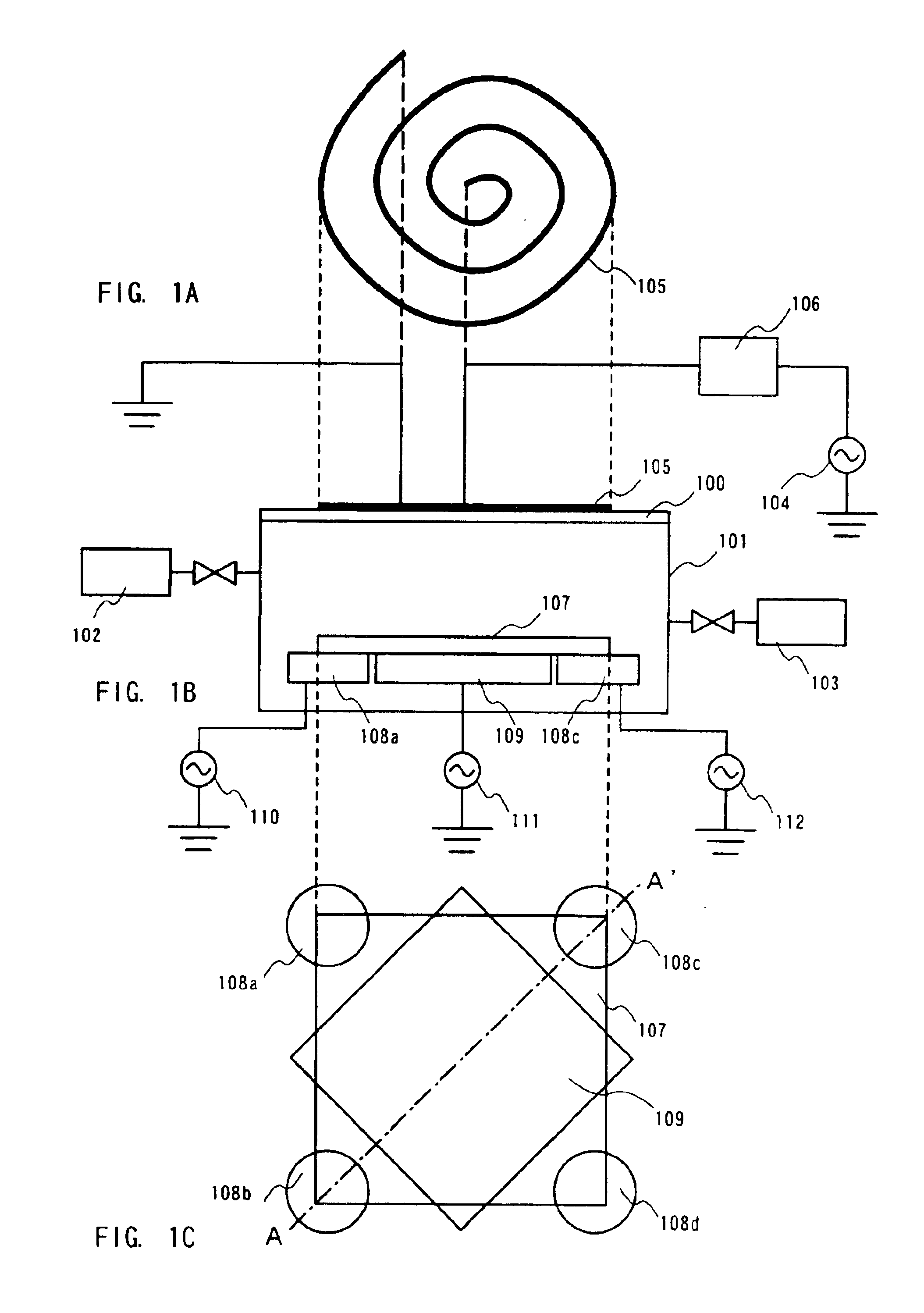
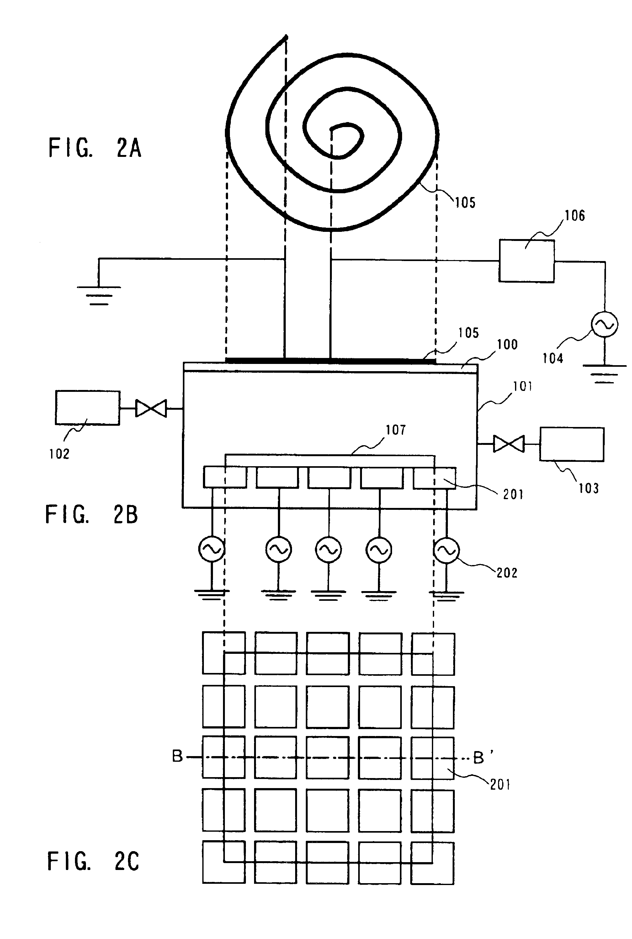
[0059]In Embodiment Mode 1, the present invention is applied to an etching apparatus using inductively coupled plasma, i.e., an ICP type etching apparatus.

[0060]FIGS. 1A to 1C show a structure of an ICP type etching apparatus. In FIG. 1B, an upper surface of a chamber 101 in the etching apparatus is made of an insulator 100 such as quartz glass, and a first electrode 105 is disposed outside the insulator 100. FIG. 1A is a top view of the first electrode 105 made of a flat coil. According to the present invention, the first electrode 105 is not limited to the shape shown in FIG. 1, and may have any shape. The first electrode 105 is connected to a first high-frequency power source 104 via a matching circuit 106. A high-frequency current flows through the first electrode 105 to form an electromagnetic wave in the chamber 101, and electrons flowing in the electromagnetic field are allowed to bump into neutral particles of a reaction gas to generate plasma. A predetermined reaction gas i...

embodiment mode 2

[0069]FIG. 3 shows an example in which the present invention is applied to a parallel-plate type etching apparatus. The parallel-plate type etching apparatus uses capacitive coupling plasma generated by applying a high frequency to electrodes through capacitors.

[0070]Reference numeral 305 denotes a first electrode (upper electrode) that is grounded. A high-frequency electric field is applied between the first electrode 305 and a second electrode to ionize a reaction gas in a chamber 301, and a material film to be etched on a substrate 307 to be treated is etched with ions in the reaction gas. A predetermined reaction gas is introduced into the chamber 301 through a gas supply system 302, and exhausted through a gas exhaust system 303.

[0071]The substrate 307 is placed on a second electrode (lower electrode) composed of a plurality of electrodes 308a to 308d, and 309 via an insulator 300 made of quartz or the like. The electrode 308a disposed below a corner portion of the substrate 30...

embodiments

Embodiment 1

[0076]In Embodiment 1, an example of a method of manufacturing a liquid crystal display apparatus provided with a pixel portion and a driving circuit on the same substrate will be described with reference to FIGS. 4A to 8.

[0077]In the present embodiment, a substrate 401 made of barium borosilicate glass or aluminoborosilicate glass (e.g., #7059 glass and #1737 glass produced by Coming Glass Corp.) is used. There is no particular limit to a substrate as long as it has light transparency. A quartz substrate may be used. A plastic substrate having heat resistance enduring a treatment temperature in the present embodiment may also be used.

[0078]An underlying insulating film 402 made of an insulating film such as a silicon oxide film, a silicon nitride film, or a silicon oxide nitride film is formed.

[0079]As the underlying insulating film 402, a silicon oxide film, a silicon nitride film, a silicon oxide nitride film (SiOxNy), a stacked film thereof, or the like can be formed...


PUM

PropertyMeasurementUnit
sizeaaaaaaaaaa
sizeaaaaaaaaaa
sizeaaaaaaaaaa

Abstract

An etching apparatus is provided, in which a plurality of electrodes are disposed for placing a substrate, high-frequency power sources as many as electrodes are provided, and the electrodes and the high-frequency power sources are connected to each other independently. Among a plurality of electrodes, a high-frequency power applied to an electrode disposed below the central portion of the substrate and a high-frequency power applied to electrodes disposed below comer portions of the substrate are controlled respectively, whereby in-plane uniformity of etching can be enhanced.

Description

BACKGROUND OF THE INVENTION[0001]1. Field of the Invention[0002]The present invention relates to a dry etching apparatus. In particular, the present invention relates to an etching apparatus using plasma generated by applying a magnetic field or an electric field to a reaction gas introduced into a low-pressure chamber, and an etching method.[0003]2. Description of the Related Art[0004]Conventionally, there is a limit to a treatment ability of a dry etching apparatus, which causes problems in terms of enhancement of productivity.[0005]In order to enhance a production efficiency, a mother glass size is increasing year after year. A currently used substrate has a size of 550 mm×650 mm, 650 mm×830 mm, etc. In the future, it is expected that a size of 850 mm×950 mm, a size of 950 mm×1000 mm, etc. will be used.[0006]Conventionally, in-plane uniformity of etching tends to decrease with an increase in size of a substrate to be treated.[0007]Japanese Patent Application Laid-open No. Hei 10-...

Claims


Application Information

Patent Timeline
Patent Type & Authority Patents(United States)
IPC IPC(8): C03C15/00H01J37/32H01L21/28G09F9/30H01L21/302H01L21/3065H01L21/311H01L21/3213H01L21/336H01L21/77H01L21/84H01L29/423H01L29/49H01L29/786
CPCC03C15/00H01J37/32009H01J37/32082H01J37/32532H01L21/31116H01L27/1214H01L29/42384H01L29/4908H01L29/66757H01L29/66765H01L29/78621H01L29/78624H01L29/78633H01L27/1259
Inventor YAMAZAKI, SHUNPEISUZAWA, HIDEOMI
Owner SEMICON ENERGY LAB CO LTD
Why Eureka
Try Eureka