Evaporation of Y-Si-O films for medium-K dielectrics

a dielectric and medium-k technology, applied in the field of semiconductor devices and device fabrication, can solve the problems of inability to meet the requirements of physical thickness and eot, gate oxides no longer have acceptable electrical properties, and current processes for depositing metal or other alternate layers on the body region of transistors, etc., to achieve the effect of increasing surface roughness

Inactive Publication Date: 2005-08-16
MICRON TECH INC
View PDF85 Cites 81 Cited by
  • Summary
  • Abstract
  • Description
  • Claims
  • Application Information

AI Technical Summary

Benefits of technology

[0014]In addition to the novel process of forming a gate oxide layer, a transistor formed by the novel process exhibits novel features that may only be formed by the novel process. Evaporation deposition of a metal, and further evaporation deposition of a metal oxide onto a body region of a transistor preserves an original smooth surface roughness of the body region in contrast to other prior deposition methods that increase surface roughness. When yttrium and silicon oxide starting materials are included, the resulting transistor fabricated with the process of this invention will exhibit a gate oxide / body region interface with a surface roughness variation as low as 0.6 nm. An equivalent oxide thickness (EOT) of less than 2 nm can be formed using the novel process described. The resulting transistor fabricated with the process of this invention further allows a gate oxide purity of 99.9999% or greater. The resulting transistor fabricated with the process of this invention further allows a yttrium-silicon oxide layer to be formed in direct interfacial contact with the body region.

Problems solved by technology

A problem with the increasing pressure of smaller transistors and lower operating voltages is that gate oxides fabricated from SiO2 are at their limit with regards to physical thickness and EOT.
Attempts to fabricate SiO2 gate oxides thinner than today's physical thicknesses show that these gate oxides no longer have acceptable electrical properties.
A problem that arises in forming an alternate oxide layer on the body region of a transistor is the process in which the alternate oxide is formed on the body region.
Current processes for depositing a metal or other alternate layer on the body region of a transistor are unacceptable due to their effect on the surface roughness of the body region.
Existing oxidation processes do not, however, repair the surface damage created by existing deposition methods such as sputtering.
Because existing methods of deposition are not capable of providing a smooth interface with an alternate material gate oxide, what is further needed is a method of forming an alternate material gate oxide that maintains a smooth interface.
At high process temperatures, materials such as dopants can also migrate to unwanted areas, changing the desired structure or composition profile that is desired.

Method used


Image

  • Evaporation of Y-Si-O films for medium-K dielectrics
  • Evaporation of Y-Si-O films for medium-K dielectrics
  • Evaporation of Y-Si-O films for medium-K dielectrics

Examples


Embodiment Construction

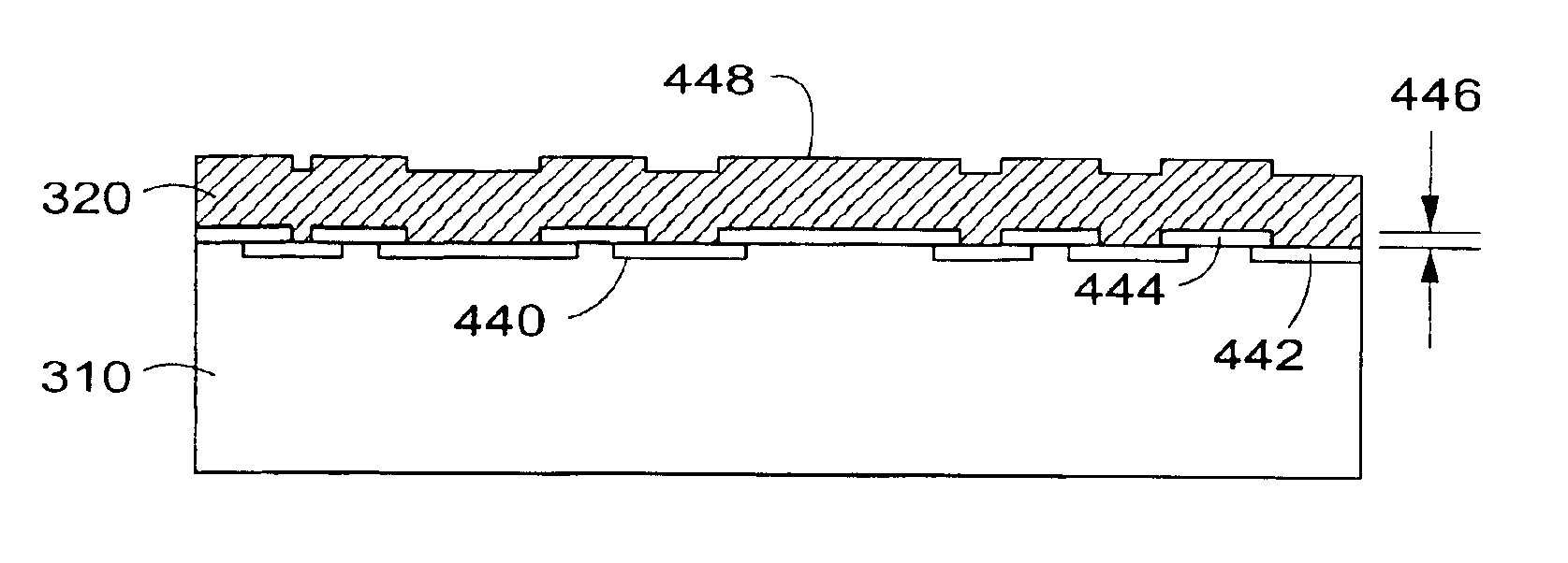
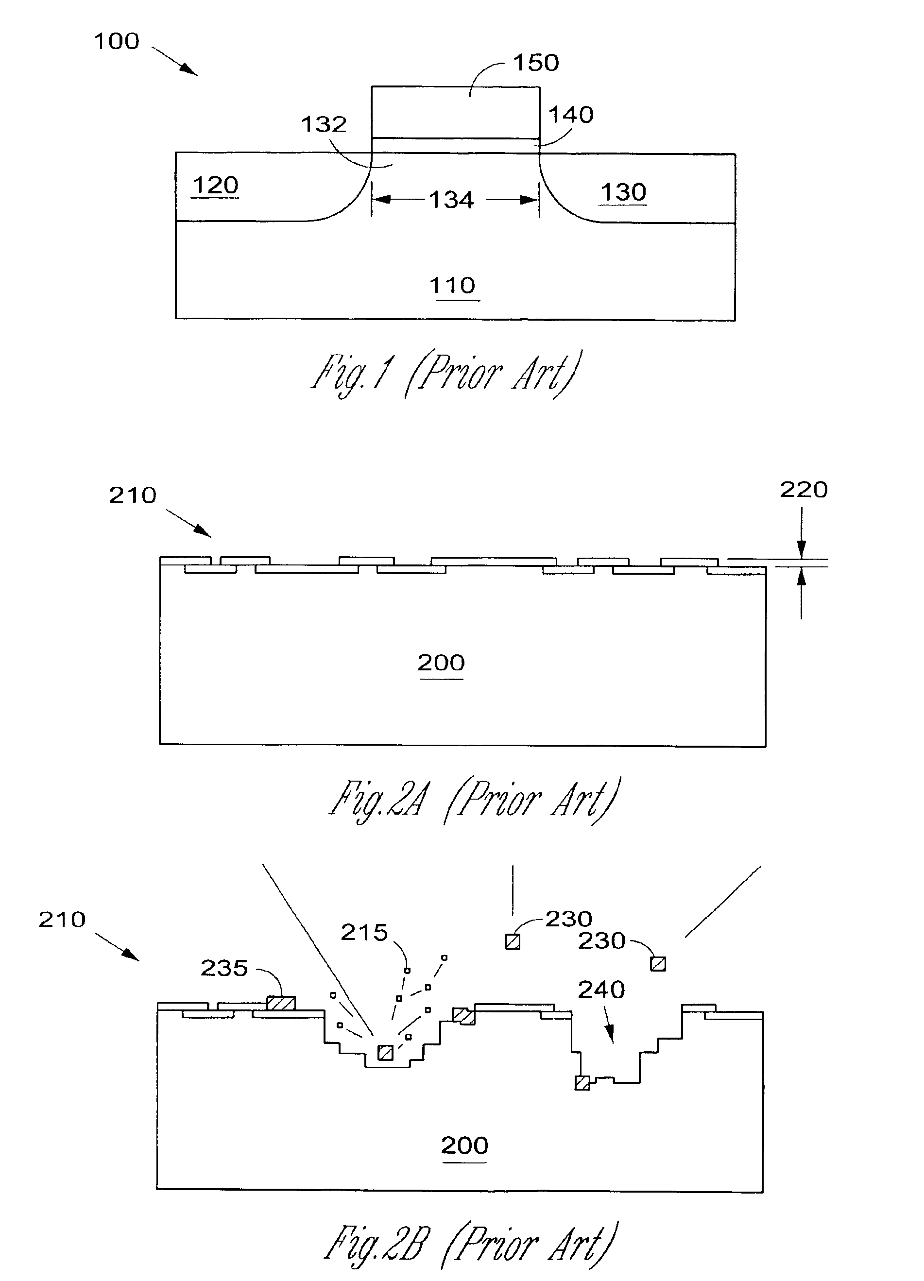
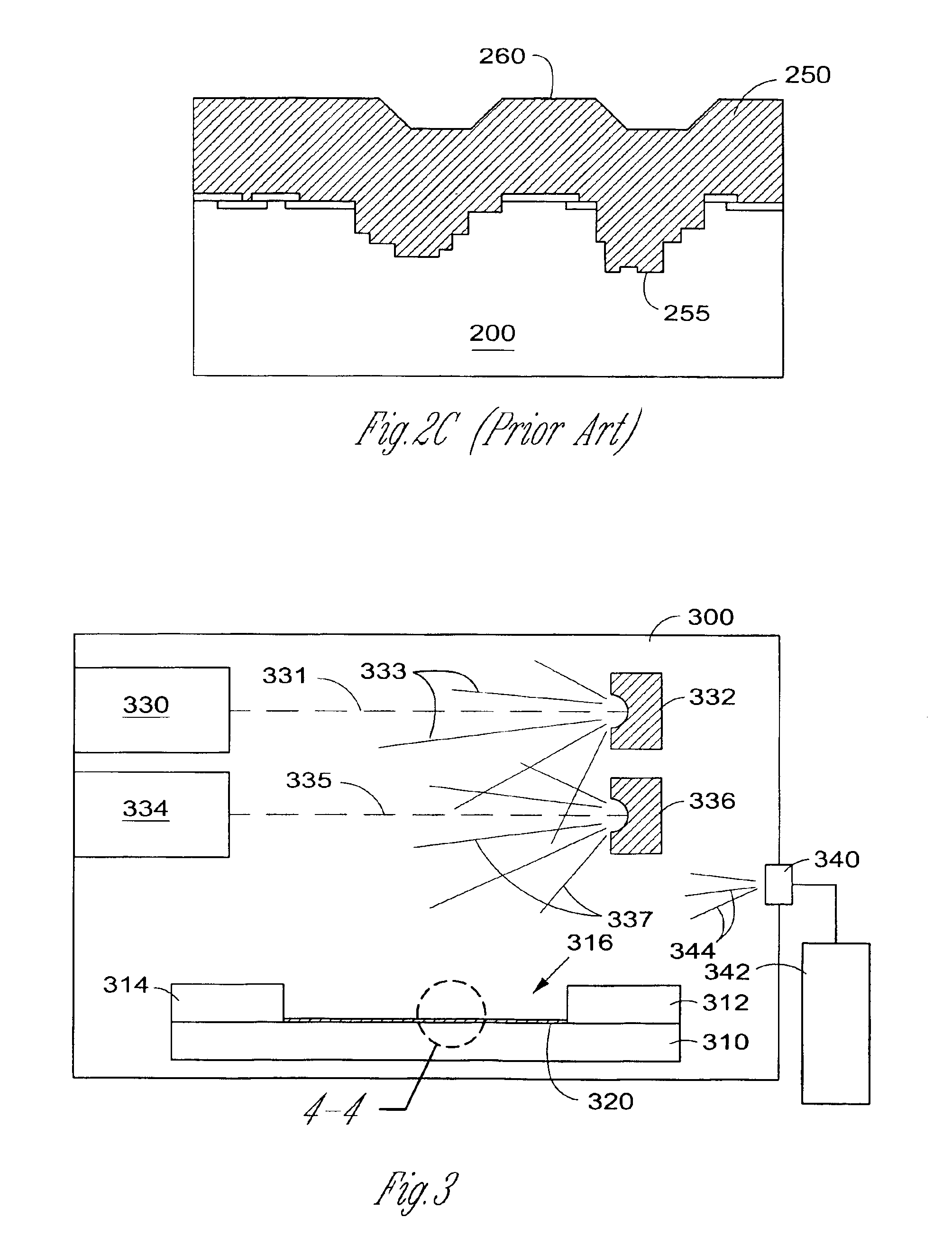
[0025]In the following detailed description of the invention, reference is made to the accompanying drawings which form a part hereof, and in which is shown, by way of illustration, specific embodiments in which the invention may be practiced. In the drawings, like numerals describe substantially similar components throughout the several views. These embodiments are described in sufficient detail to enable those skilled in the art to practice the invention. Other embodiments may be utilized and structural, logical, and electrical changes may be made without departing from the scope of the present invention. The terms wafer and substrate used in the following description include any structure having an exposed surface with which to form the integrated circuit (IC) structure of the invention. The term substrate is understood to include semiconductor wafers. The term substrate is also used to refer to semiconductor structures during processing, and may include other layers that have be...


PUM

PropertyMeasurementUnit
surface roughnessaaaaaaaaaa
dielectric constantaaaaaaaaaa
thicknessaaaaaaaaaa

Abstract

A gate oxide and method of fabricating a gate oxide that produces a more reliable and thinner equivalent oxide thickness than conventional SiO2 gate oxides are provided. Gate oxides formed from yttrium, silicon, and oxygen are thermodynamically stable such that the gate oxides formed will have minimal reactions with a silicon substrate or other structures during any later high temperature processing stages. The process shown is performed at lower temperatures than the prior art, which inhibits unwanted species migration and unwanted reactions with the silicon substrate or other structures. Using a thermal evaporation technique to deposit the layer to be oxidized, the underlying substrate surface smoothness is preserved, thus providing improved and more consistent electrical properties in the resulting gate oxide.

Description

RELATED APPLICATIONS[0001]This application is a divisional of U.S. application Ser. No. 10 / 099,194 filed Mar. 13, 2002 now U.S. Pat. No. 6,812,100 which is incorporated herein by reference.FIELD OF THE INVENTION[0002]The invention relates to semiconductor devices and device fabrication. Specifically, the invention relates to gate oxide layers of transistor devices and their method of fabrication.BACKGROUND OF THE INVENTION[0003]In the semiconductor device industry, particularly in the fabrication of transistors, there is continuous pressure to reduce the size of devices such as transistors. The ultimate goal is to fabricate increasingly smaller and more reliable integrated circuits (ICs) for use in products such as processor chips, mobile telephones, or memory devices such as DRAMs. The smaller devices are frequently powered by batteries, where there is also pressure to reduce the size of the batteries, and to extend the time between battery charges. This forces the industry to not ...

Claims


Application Information

Patent Timeline
Patent Type & Authority Patents(United States)
IPC IPC(8): H01L21/02H01L21/28H01L29/51H01L21/316H01L29/40
CPCH01L21/28194H01L21/31604H01L29/517H01L21/02263
Inventor AHN, KIE Y.FORBES, LEONARD
Owner MICRON TECH INC
Why Eureka
Try Eureka