Semiconductor device and manufacturing method of the same

a technology of semiconductor devices and impurity atoms, which is applied in the direction of semiconductor devices, radio frequency controlled devices, electrical apparatus, etc., can solve the problems of large diffusion coefficient of impurity atoms, insufficient concentration of electrically active impurity atoms, and difficulty in forming high carrier concentrations in deep channel regions. , to achieve the effect of suppressing the diffusion of impurity atoms and improving the activation rate of impurity atoms

Inactive Publication Date: 2005-08-16
KK TOSHIBA
View PDF5 Cites 138 Cited by
  • Summary
  • Abstract
  • Description
  • Claims
  • Application Information

AI Technical Summary

Benefits of technology

[0009]An object of the present invention is to provide a semiconductor device having a doping layer so as to improve an activation rate of an impurity atom and to suppress diffusion of the impurity atom.

Problems solved by technology

However, depending on a doping impurity atom, an insufficient concentration of an electrically active impurity atom is provided.
Alternatively, the desired impurity distribution is not provided which results in a large diffusion coefficient of the impurity atom.
However, it is difficult to form a high carrier concentration in a deep channel region because of a low active impurity concentration of In.
However, it is very difficult to form a shallow impurity diffusion layer so that a diffusion coefficient of B in a Si crystal is large.
Further, because of the low active impurity concentration, In cannot be used as an acceptor impurity atom of the source / drain region of the p-channel MOSFET.
However, a carrier concentration cannot exceed the active impurity concentration of P and As.
However, it is impossible to achieve a higher carrier concentration exceeding the active impurity concentration of the dopant atom.
It is also impossible to suppress the diffusion of the heavily doped impurity atom.

Method used


Image

  • Semiconductor device and manufacturing method of the same
  • Semiconductor device and manufacturing method of the same
  • Semiconductor device and manufacturing method of the same

Examples


Embodiment Construction

[0020]Various embodiments of the present invention will be described with reference to the accompanying drawings. It is to be noted that the same or similar reference numerals are applied to the same or similar parts and elements throughout the drawings, and the description of the same or similar parts and elements will be omitted or simplified.

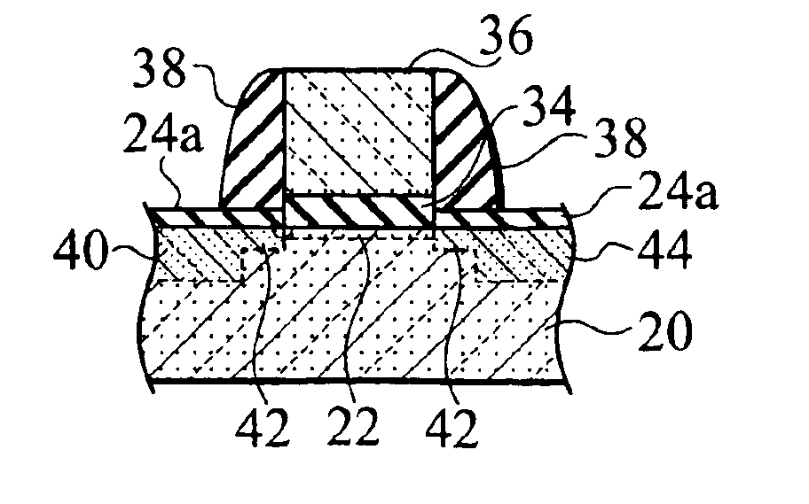
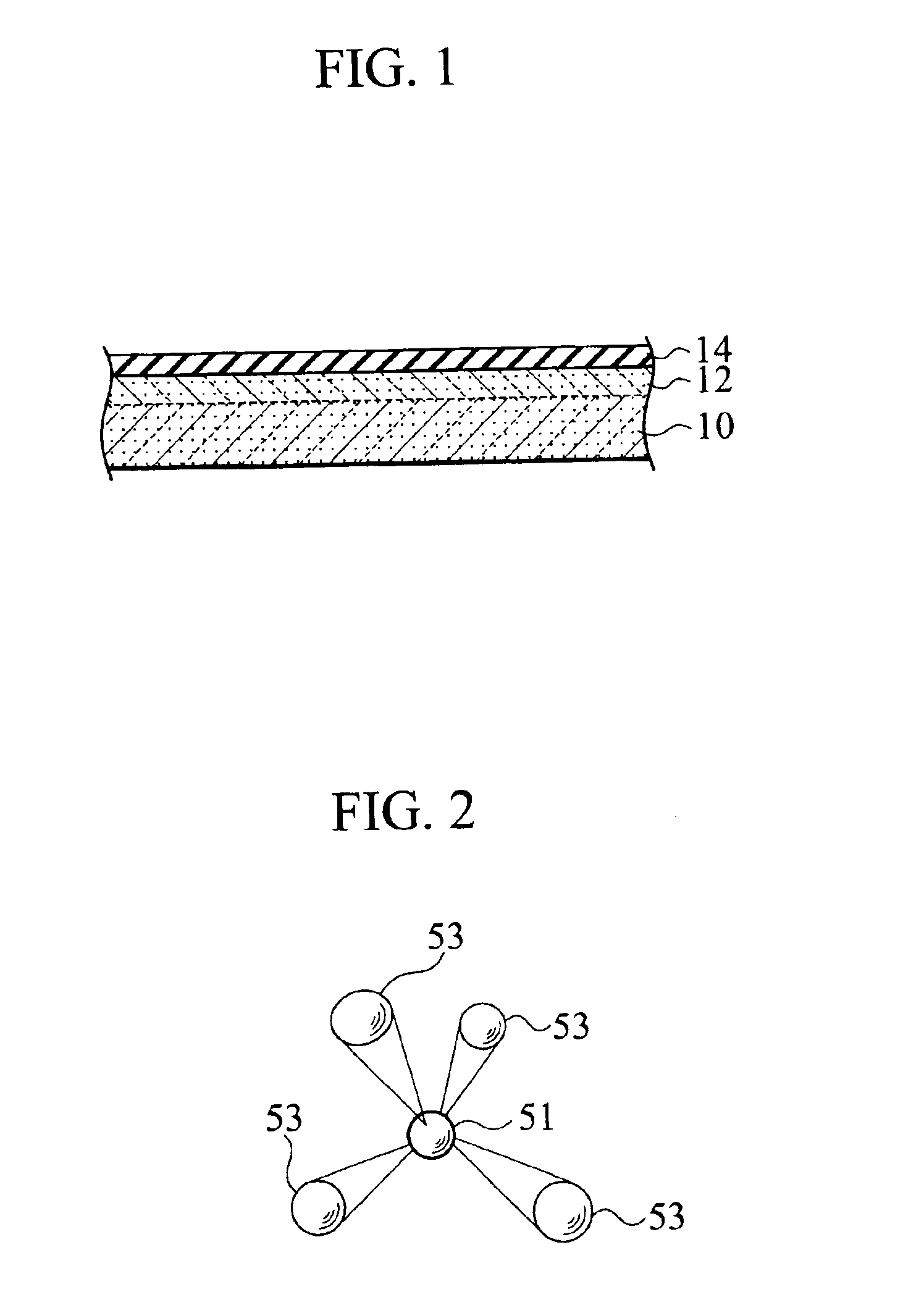
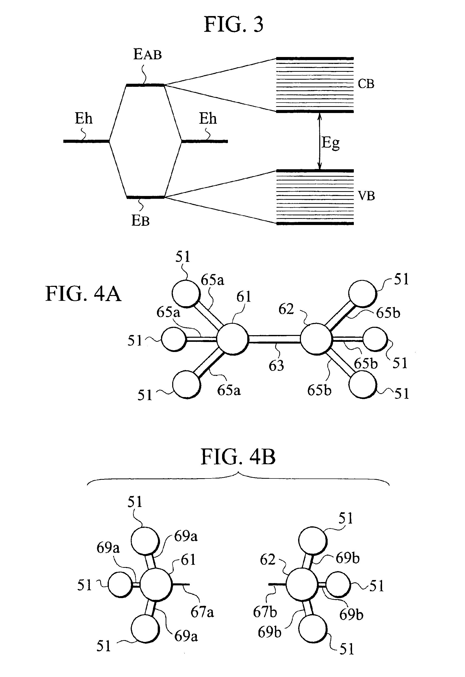
[0021]A semiconductor device according to an embodiment of the present invention includes, as shown in FIG. 1, a semiconductor layer 12 doped with first and second impurity atoms by a nearest neighbor lattice site location in a principal surface side of a semiconductor substrate 10. On the semiconductor layer 12, for example, an insulating film 14 such as a gate oxide film of the semiconductor device is deposited. For example, a covalent bond radius of the first impurity atom is larger than the minimum of a covalent bond radius of a constituent atom of the semiconductor layer 12, and a covalent bond radius of the second impurity atom is small...


PUM


Abstract

A semiconductor device having a semiconductor layer, includes: a first impurity atom having a covalent bond radius larger than a minimum radius of a covalent bond of a semiconductor constituent atom of a semiconductor layer; and a second impurity atom having a covalent bond radius smaller than a maximum radius of the covalent bond of the semiconductor constituent atom; wherein the first and second impurity atoms are arranged in a nearest neighbor lattice site location and at least one of the first and second impurity atoms is electrically active.

Description

CROSS REFERENCE TO RELATED APPLICATIONS[0001]This application is based upon and claims the benefit of priority from prior Japanese Patent Application P2002-278088 filed on Sep. 24, 2002; the entire contents of which are incorporated by reference herein.BACKGROUND OF THE INVENTION[0002]1. Field of the Invention[0003]The present invention relates to a semiconductor device and a manufacturing method for the same. In particular, it relates to a semiconductor device using a semiconductor layer doped with impurity atoms having different covalent bond radii.[0004]2. Description of the Related Art[0005]Control of an impurity distribution in a semiconductor layer is extremely important for a semiconductor device. Generally, a thermal diffusion process is used as a technique to form an impurity distribution in a semiconductor layer with high controllability. However, depending on a doping impurity atom, an insufficient concentration of an electrically active impurity atom is provided. Alterna...

Claims


Application Information

Patent Timeline
Patent Type & Authority Patents(United States)
IPC IPC(8): H01L21/02H01L21/265H01L21/22H01L27/148H01L21/24H01L29/78H01L29/12H01L29/02H01L29/772H01L29/66H01L21/336H01L21/425
CPCH01L29/6659H01L21/2652H01L21/26566H01L21/24
Inventor YAMAUCHI, JUNAOKI, NOBUTOSHI
Owner KK TOSHIBA
Why Eureka
Try Eureka