

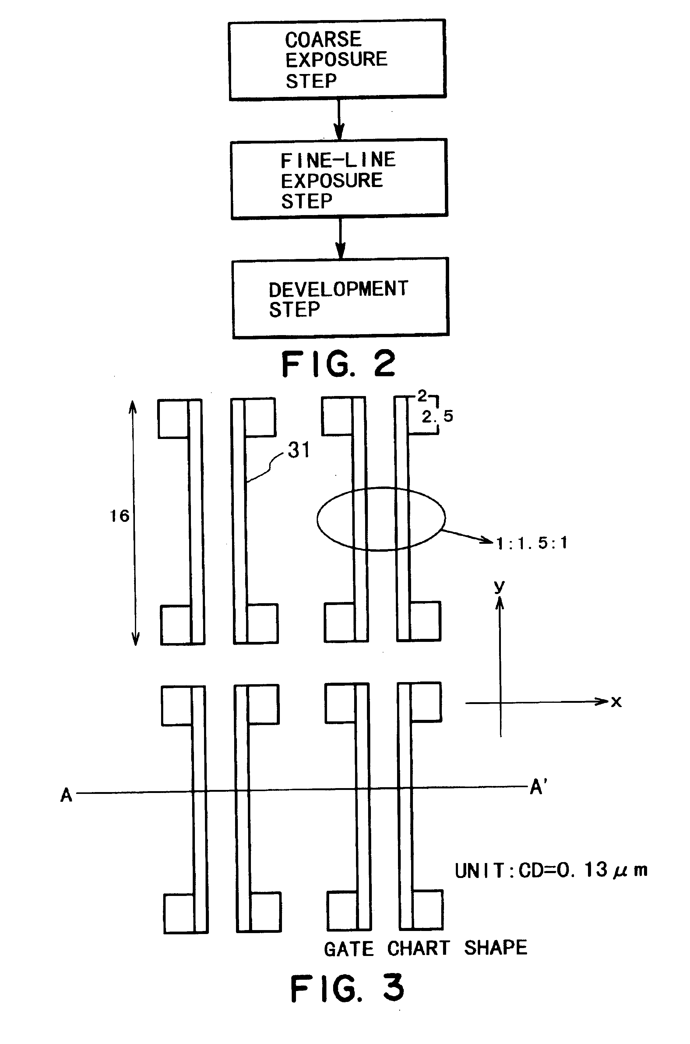
Multiple exposure method
a multi-exposure, exposure method technology, applied in the direction of microlithography exposure apparatus, printers, instruments, etc., can solve the problems of difficult to form a pattern of 0.15 micron or less, difficult to develop a practical glass material, critical problem of wavelength shortening, etc., to achieve the effect of short tim
- Summary
- Abstract
- Description
- Claims
- Application Information
AI Technical Summary
Benefits of technology
Problems solved by technology
Method used
Image

Examples
first embodiment
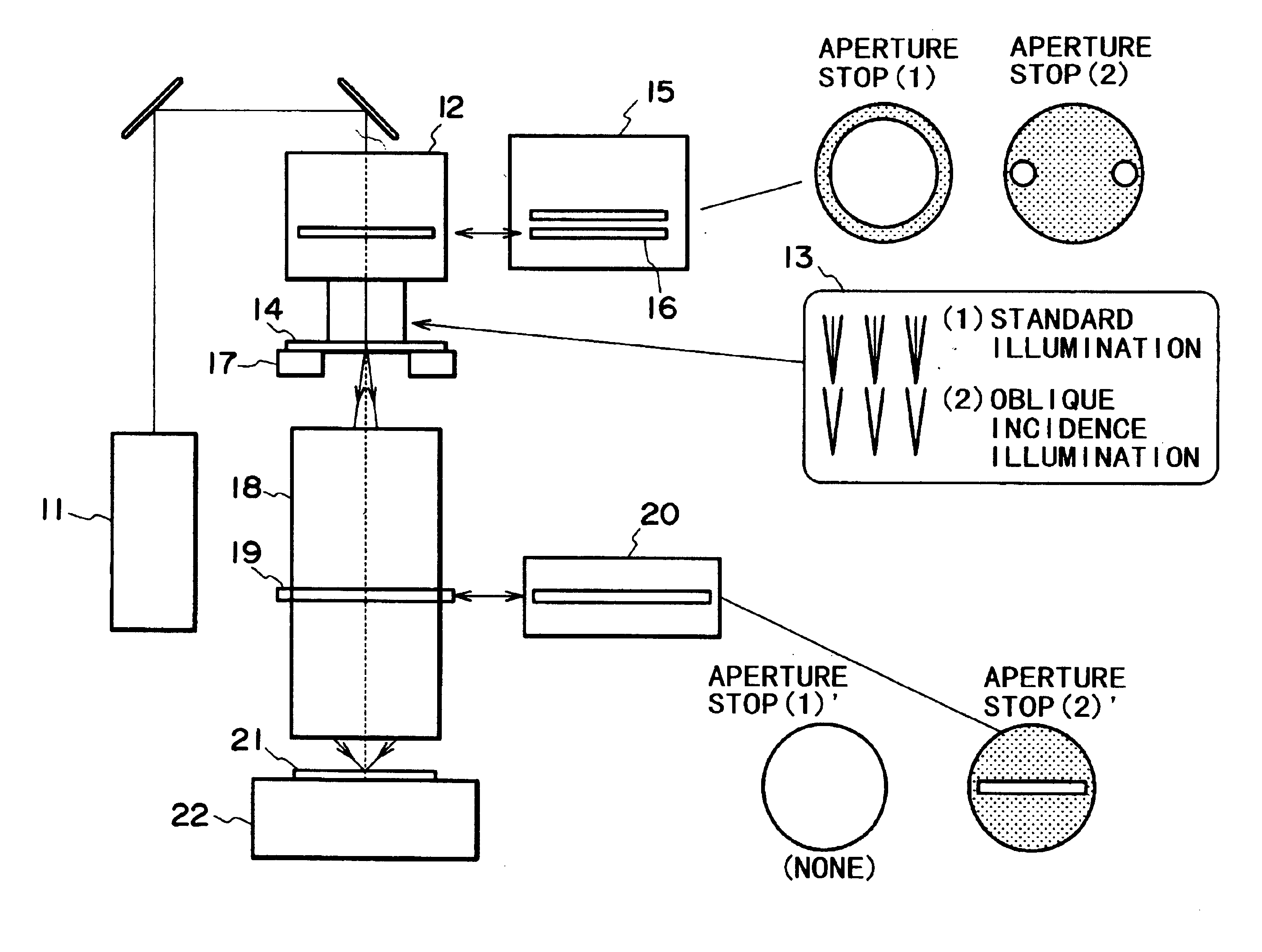
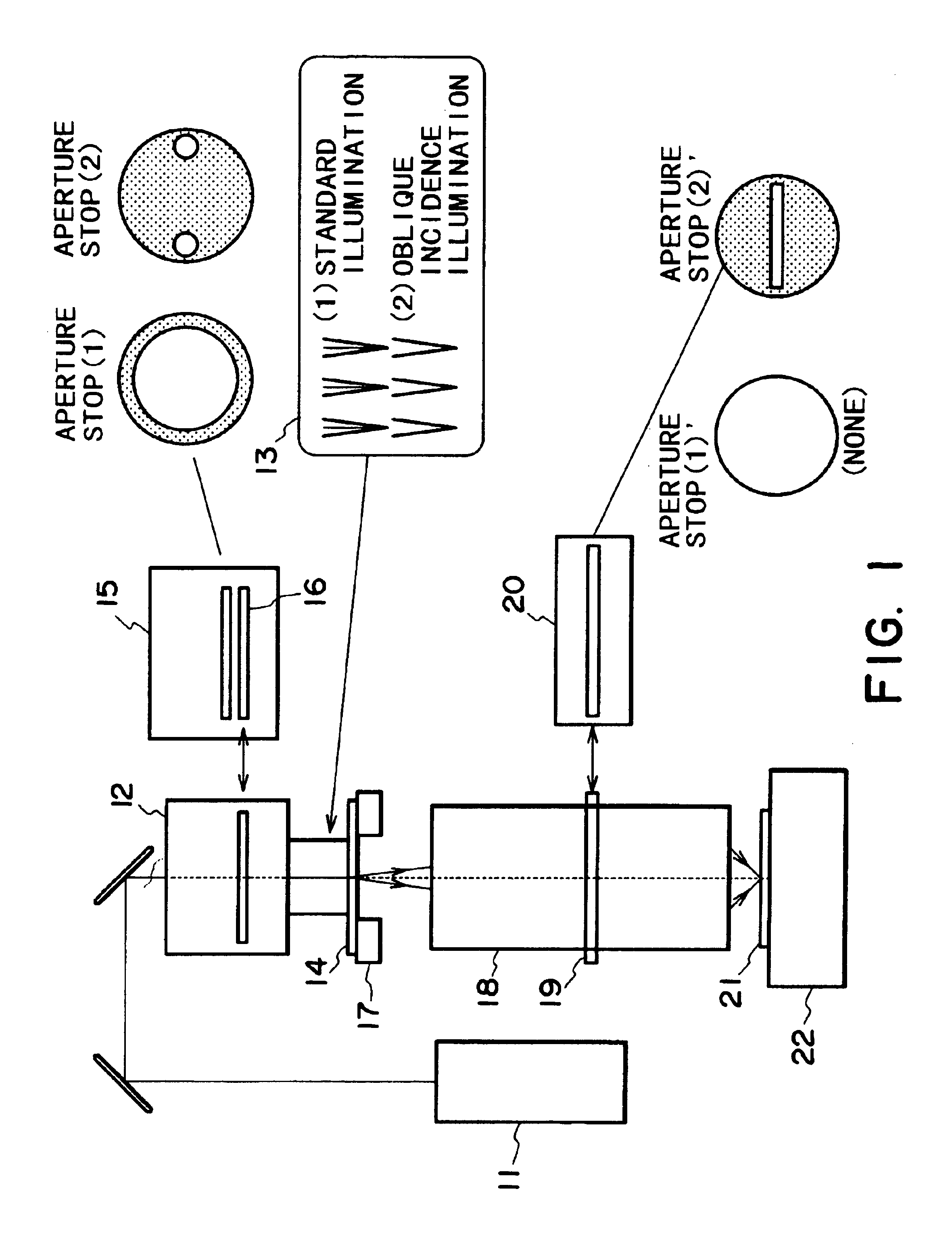
[0129]the present invention will be described below.
[0130]The first embodiment has a feature that, in a projection exposure apparatus, the illumination condition of an illumination optical system and an aperture stop of a projection optical system are changed in operational association with each other.
[0131]In accordance with this embodiment, a projection exposure apparatus is equipped with an illumination condition changing mechanism and an aperture stop changing mechanism, which may be similar to those used conventionally. Therefore, the present embodiment does not need a large modification of the structure. Further, the multiple exposure process of this embodiment needs, basically, only a single mask which can be produced by patterning similar to conventional masks, with only a small modification. The manufacturing cost is, therefore, not large.
[0132]This embodiment does not use an exclusive dual-beam interferometer. Also, there is no necessity of using, in a projection exposure ...
PUM
| Property | Measurement | Unit |
|---|---|---|
| size | aaaaa | aaaaa |
| angle | aaaaa | aaaaa |
| angle | aaaaa | aaaaa |
Abstract
Description
Claims
Application Information