Electron beam exposure apparatus and semiconductor device manufacturing method

Inactive Publication Date: 2005-08-16
CANON KK
7 Cites 5 Cited by

AI-Extracted Technical Summary

Problems solved by technology

Additionally, a conventional stage has certain constraints, i.e., the stage must be arranged in a vacuum chamber and is not allowed to cause any variation in magnetic field, which may affect the positioning of electron beams.
However, a contact mechanical element suffers from problems about lubrication, particles, and the like.
Even with this method, a correction control system using a deflector...

Method used

[0059]The θ linear motor movable element 106 and θ linear motor stator 106′ are preferably coated with multiple electromagnetic shields. For this reason, a magnet serving as the θ linear motor movable element 106 is preferably coated with multiple electromagnetic shields of, e.g., permalloy to avoid any variation in the magnetic field. In addition, the magnet serving as the θ linear motor movable element 106 is preferably spaced apart from the reduction electron optical system 4 by a sufficient distance to avoid any variation in magnetic field due to a leakage magnetic field from the reduction electron optical system 4. More specifically, the θ linear motor movable element 106 and the wafer 5 are desirably located on the opposite sides of the barycenter of the center slider 12 in the Z-axis direction. The θ linear motor stator 106′ may be arranged on the tilt frame 13.
[0062]As described above, according to this embodiment, the electromagnetic actuator is provided between the substrate stage and the transfer stage. With this arrangement, the substrate stage can be driven in a non-contact manner in at least the rotation direction about the Z-axis, thus preventing vibrations from being transmitted from the transfer stage to the substrate stage. For this reason, stages (the substrate stage and transfer stage) having high-frequency band control characteristics with respect to the rotation direction about the Z-axis can be implemented. Consequently, in an electron beam exposure apparatus having these stages, especially in an electron beam exposure apparatus using a plurality of electron beams, a degradation in drawing accuracy caused by a yawing component generated in stage scanning can be reduced, and high-accuracy exposure can be realized.
[0065]In this embodiment, the tilt frame 13 shown in FIG. 2 is not always necessary. Since the linear motor movable elements and linear motor stators are in non-contact with each other, the substrate stage can be driven in a non-contact manner. It is thermally preferable that each linear motor movable element comprises a magnet, and each linear motor stator comprises a coil. Each electromagnetic actuator is preferably coated with multiple electromagnetic shields. For this reason, a magnet serving as the linear motor movable element is preferably coated with multiple electromagnetic shields of, e.g., permalloy to avoid any variation in magnetic field. In addition, the magnet serving as the linear motor movable element is preferably spaced apart from a reduction electron optical system 4 by a sufficient distance to avoi...

Benefits of technology

[0017]The present invention has been made in consideration of the above-mentioned problems, and has as its object to provide a...

Abstract

An electron beam exposure apparatus which exposes a substrate with a predetermined pattern using one or a plurality of electron beams. The apparatus includes a substrate stage on which a substrate is mounted, a transfer stage which drives the substrate stage on an X-Y plane, an electromagnetic actuator which drives the substrate stage in a rotation direction about a Z-axis with respect to the transfer stage, and a measuring system which measures a position of the substrate stage in the rotation direction about the Z-axis using a measuring beam along a direction perpendicular to the plurality of electron beams.

Application Domain

Technology Topic

Image

  • Electron beam exposure apparatus and semiconductor device manufacturing method
  • Electron beam exposure apparatus and semiconductor device manufacturing method
  • Electron beam exposure apparatus and semiconductor device manufacturing method

Examples

  • Experimental program(3)

Example

[First Embodiment]
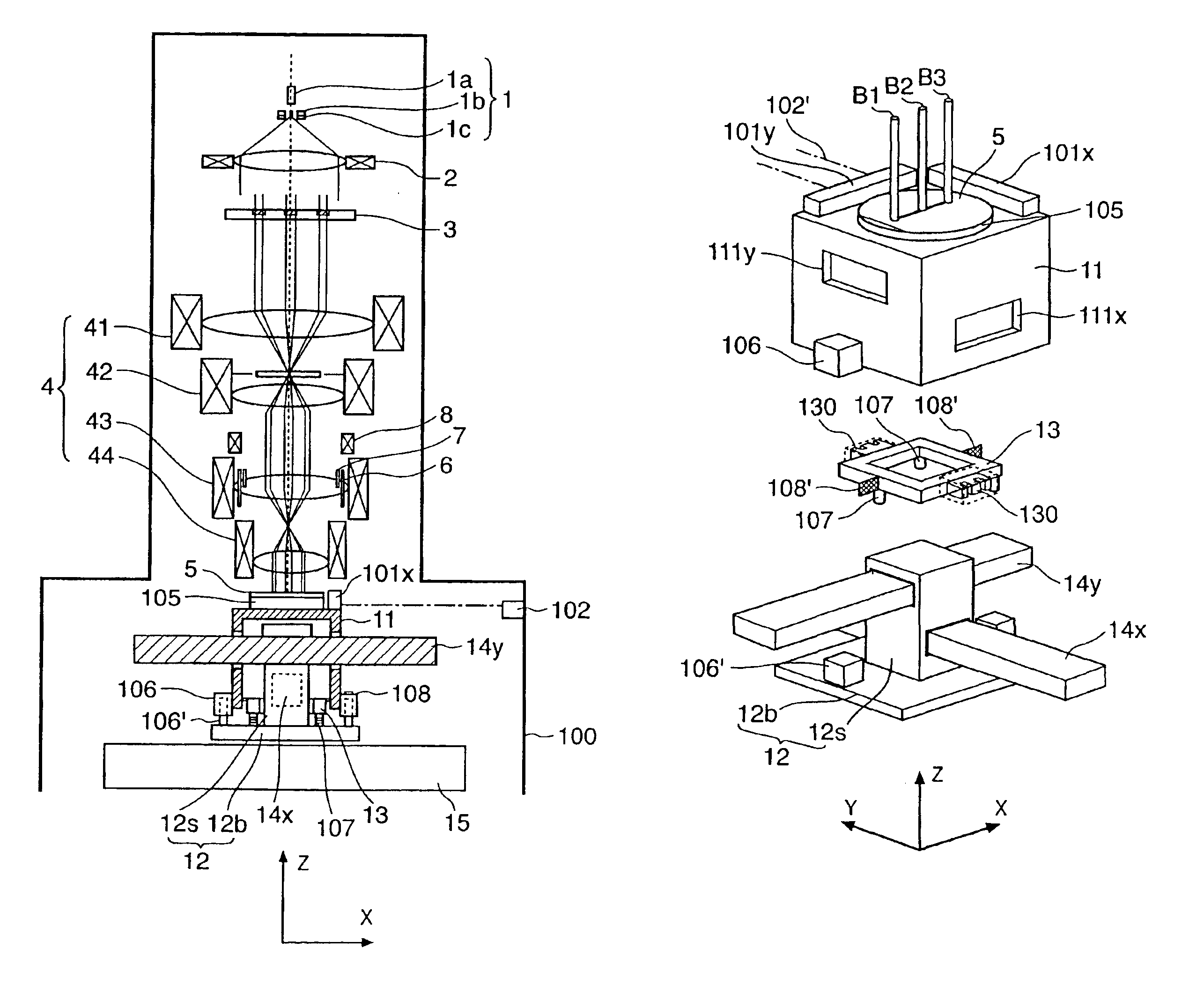
[0045]FIG. 1 is a view showing an electron beam exposure apparatus according to a preferred embodiment of the present invention.
[0046]An electron gun 1 comprises a cathode 1a, grid 1b, and anode 1c. Electrons emitted from the cathode 1a form a crossover image between the grid 1b and anode 1c (this crossover image will be referred to as a light source hereinafter).
[0047]Electrons emitted from the light source form a substantially parallel electron beam through a condenser lens 2, whose front focal position is located at the light source position. The substantially parallel electron beam comes incident on an element electron optical system array 3. The element electron optical system array 3 is formed by arranging a plurality of element electron optical systems, each comprising a blanking electrode, an aperture, and an electron lens, in a direction perpendicular to the optical axis parallel to the Z-axis. The element electron optical system array 3 will be described in detail later.
[0048]The element electron optical system array 3 forms a plurality of intermediate images of the light source. The respective intermediate images are reduced and projected onto a wafer 5 serving as a substrate by a reduction electron optical system 4 (to be described later), to form light source images on the wafer 5. The respective elements of the element electron optical system array 3 are set such that the spacing between adjacent light source images on the wafer 5 is an integer multiple of the size of each light source image. Additionally, in the element electron optical system array 3, the position of each intermediate image in the direction of the optical axis is differently adjusted in accordance with the curvature of field of the reduction electron optical system 4. The element electron optical system array 3 also corrects, in advance, an aberration that occurs when each intermediate image is reduced and projected onto the wafer 5 by the reduction electron optical system 4.
[0049]The reduction electron optical system 4 comprises a symmetric magnetic tablet including a first projection lens 41 (43) and a second projection lens 42 (44). The distance between the two lenses 41 and 42 is f1+f2 where f1 is the focal length of the first projection lens 41 (43) and f2 is the focal length of the second projection lens 42 (44). The object point on the optical axis is at the focal position of the first projection lens 41 (43), and the image point on the optical axis is formed on the focal point of the second projection lens 42 (44). This image is reduced to f2/f1. The two lens magnetic fields are determined to act in the opposite directions. Hence, theoretically, Seidel aberrations other than five aberrations, i.e., spherical aberration, isotropic astigmatism, isotropic coma, curvature of field, and on-axis chromatic aberration, and chromatic aberrations concerning rotation and magnification are cancelled.
[0050]A deflector 6 deflects a plurality of electron beams from the element electron optical system array 3 to displace a plurality of light source images on the wafer 5 by substantially the same displacement amount in the X- and Y-axis directions. The deflector 6 includes a main deflector, which is used when a deflection width is large, and a subdeflector, which is used when the deflection width is small (both not shown). The main deflector is an electromagnetic deflector, while the subdeflector is an electrostatic deflector.
[0051]A dynamic focus coil 7 corrects the focal position shift of a light source image formed by the deflection aberration that occurs when the deflector 6 is actuated. A dynamic stigmatic coil 8 corrects deflection aberration caused by deflection, i.e., astigmatism, in the same manner as the dynamic focus coil 7.
[0052]A θZ tilt stage 11 serving as a substrate stage has a wafer 5 on it and can move in the direction of the optical axis (direction substantially parallel to the Z-axis), the rotation direction (θ direction) about the Z-axis, and the tilt direction.
[0053]An X-Y transfer stage 12 (to be referred to as a center slider hereinafter) serving as a transfer stage moves on a stage base 15 and drives the θZ tilt stage 11 in the X and Y directions.
[0054]FIG. 2 is a view showing in detail the stage (the θZ tilt stage 11 and center slider 12) used in the electron beam exposure apparatus of FIG. 1. As shown in FIG. 2, the θZ tilt stage 11 comprises a substrate holder 105 which holds, e.g., the wafer 5 on its surface and reflection mirrors 101x and 101y for position measurement. The θZ tilt stage 11 has a cage structure surrounding the center slider 12 and has apertures 111x and 111y, through which an X movable guide 14x and a Y movable guide 14y extend.
[0055]The position of the θZ tilt stage 11 in the X and Y directions is measured by, e.g., a laser interferometer 102 held by a sample chamber 100 shown in FIG. 1, with reference to the inner wall of the sample chamber 100. By using the reflection mirrors 101x and 101y, the θZ tilt stage 11 is also measured in the θ and tilt directions. θ measurement 102′ is preferably performed from a side perpendicular to the array of a plurality of beams. The position in the Z-axis direction is detected by an optical sensor with non-photosensitive light. As a servo sensor, a vacuum encoder may be employed.
[0056]As shown in FIG. 2, the center slider 12 can move in the X and Y directions on the X-Y plane, which is perpendicular to the direction (substantially parallel to the Z-axis) of the optical axis and parallel to the stage base 15. As the center slider 12, an X-Y transfer stage as shown in FIG. 4 can also be used.
[0057]The center slider 12 will be described in detail with reference to FIG. 5. The center slider 12 comprises a bottom plate 12b and side plates 12s. Below the bottom plate 12b, bearings are arranged on the stage base 15 to face each other. Inside the side plates 12s, the X movable guide 14x and Y movable guide 14y are sandwiched between bearings.
[0058]As shown in FIG. 2, a θ linear motor movable element 106, which constitutes a part of an electromagnetic actuator and a θ linear motor stator 106′, which constitutes the remainder of the electromagnetic actuator, are provided between the θZ tilt stage 11 and the center slider 12. The θ linear motor movable element 106 and θ linear motor stator 106′ drive the θZ tilt stage 11 in at least the rotation direction about the Z-axis with respect to the center slider 12. More specifically, the θ linear motor movable element 106 is fixed at the end of the θZ tilt stage 11, and the θ linear motor stator 106′, is fixed on the bottom plate 12b of the transfer stage 12 to face the θ linear motor movable element 106. Since the θ linear motor movable element 106 and θ linear motor stator 106′ are in non-contact with each other, the substrate stage can be driven in a non-contact manner. From a thermal viewpoint, it is preferable that the θ linear motor movable element 106 comprises a magnet, and the θ linear motor stator 106′ comprises a coil.
[0059]The θ linear motor movable element 106 and θ linear motor stator 106′ are preferably coated with multiple electromagnetic shields. For this reason, a magnet serving as the θ linear motor movable element 106 is preferably coated with multiple electromagnetic shields of, e.g., permalloy to avoid any variation in the magnetic field. In addition, the magnet serving as the θ linear motor movable element 106 is preferably spaced apart from the reduction electron optical system 4 by a sufficient distance to avoid any variation in magnetic field due to a leakage magnetic field from the reduction electron optical system 4. More specifically, the θ linear motor movable element 106 and the wafer 5 are desirably located on the opposite sides of the barycenter of the center slider 12 in the Z-axis direction. The θ linear motor stator 106′ may be arranged on the tilt frame 13.
[0060]The center slider 12 has the X movable guide 14x and Y movable guide 14y arranged in the shape of a cross. The center slider 12 moves smoothly along the side surface of the Y movable guide 14y and the upper surface of the stage base 15 in the X-axis direction by moving the X movable guide 14x in the X-axis direction and moves smoothly along the side surface of the X movable guide 14x and the upper surface of the stage base 15 in the Y-axis direction by moving the Y movable guide 14y in the Y-axis direction.
[0061]The tilt frame 13 is supported through Z actuators 107 for driving the θZ tilt stage 11 above the bottom plate 12b of the center slider 12 in the Z direction. As the Z actuators 107, piezoelectric devices with guides which are rigid in the X-Y plane may be used. The tilt frame 13 has θ free leaf springs 108, each serving as a connecting member with a degree of freedom in only the θ direction (rotation direction about the Z-axis). The θZ tilt stage 11 is supported by the tilt frame 13 through the θ free leaf springs 108. Some of the θ free leaf springs 108 are arranged in the X-axis direction, and the others, in the Y-axis direction. The θZ tilt stage 11 is rigid with respect to the tilt frame 13 in the Z-axis direction. The tilt frame 13 is arranged to surround the center slider 12.
[0062]As described above, according to this embodiment, the electromagnetic actuator is provided between the substrate stage and the transfer stage. With this arrangement, the substrate stage can be driven in a non-contact manner in at least the rotation direction about the Z-axis, thus preventing vibrations from being transmitted from the transfer stage to the substrate stage. For this reason, stages (the substrate stage and transfer stage) having high-frequency band control characteristics with respect to the rotation direction about the Z-axis can be implemented. Consequently, in an electron beam exposure apparatus having these stages, especially in an electron beam exposure apparatus using a plurality of electron beams, a degradation in drawing accuracy caused by a yawing component generated in stage scanning can be reduced, and high-accuracy exposure can be realized.

Example

[Second Embodiment]
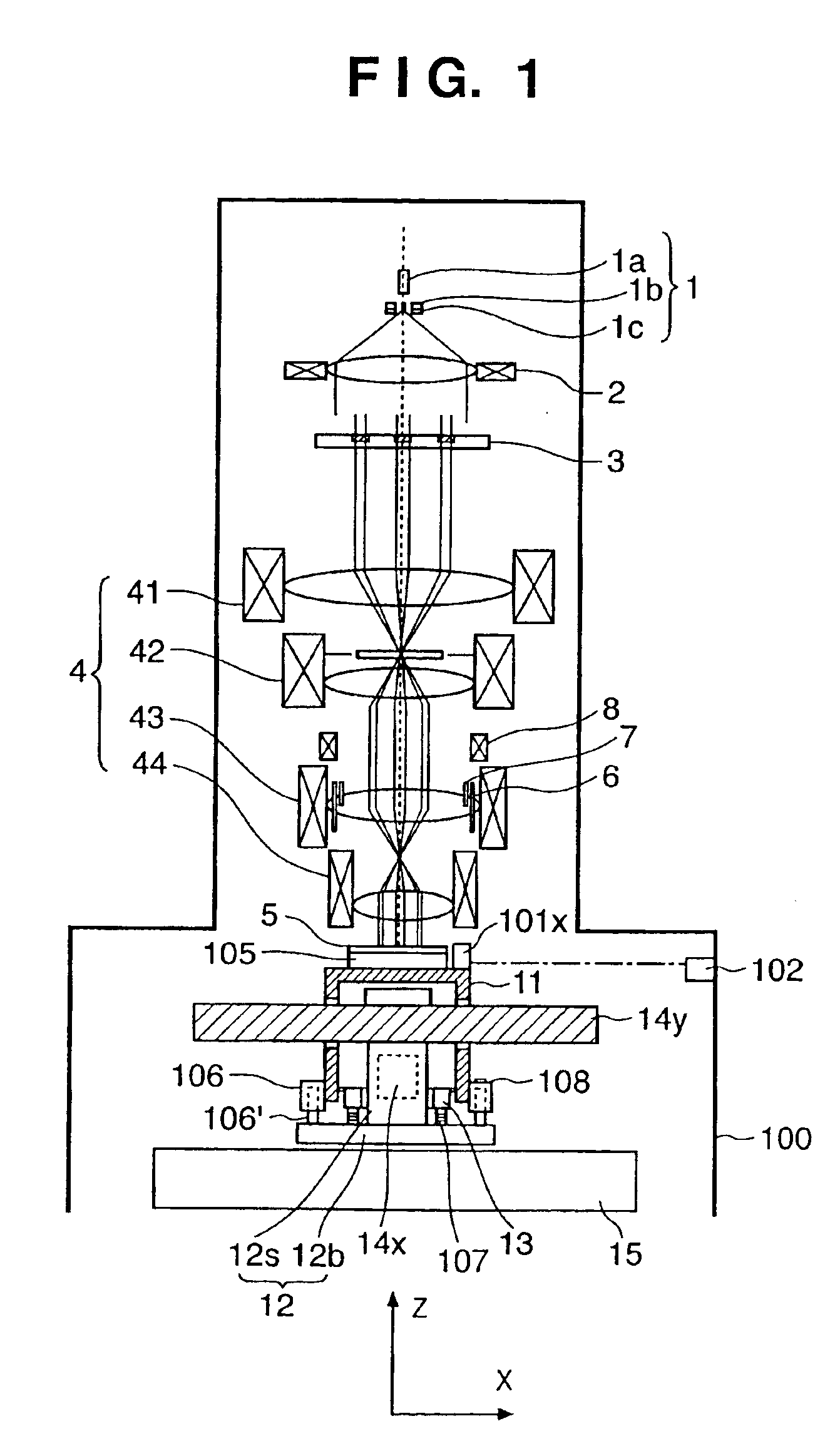
[0063]FIGS. 3A and 3B are views showing an electron beam exposure apparatus according to the second embodiment of the present invention.
[0064]In this embodiment, a plurality of electromagnetic actuators are combined. With this arrangement, a θZ tilt stage 11 can be driven with six degrees of freedom. As shown in FIG. 3A, the θZ tilt stage 11 has a cage structure surrounding a center slider 12 and has apertures 111x and 111y, through which an X movable guide 14x and a Y movable guide 14y extend. Six linear motor movable elements 120x, 120y, and 120z, which constitute parts of respective electromagnetic actuators, are fixed on the side surface of the θZ tilt stage 11. Linear motor stators 120x′, 120y′, and 120z′, which constitute the remainders of the respective electromagnetic actuators, are fixed on a bottom plate 12b to face the linear motor movable elements 120x, 120y, and 120z, respectively. As shown in FIG. 3B, the driving directions of the respective linear motors as electromagnetic actuators are determined by the three linear motor movable elements 120z, which generate a driving force in the Z-axis direction, the two linear motor movable elements 120x, which generate a driving force in the X-axis and θ (rotation direction about the Z-axis) directions, and one linear motor movable element 120y, which generates a driving force in the Y-axis direction. An electromagnetic actuator which generates a driving force in the rotation direction about the X-axis and one which generates a driving force in the rotation direction about the Y-axis may also be provided in the same manner. As described above, since a plurality of linear motors for a plurality of directions are combined, the θZ tilt stage 11 can be driven with six degrees of freedom. A method of combining linear motors, however, is not limited to this.
[0065]In this embodiment, the tilt frame 13 shown in FIG. 2 is not always necessary. Since the linear motor movable elements and linear motor stators are in non-contact with each other, the substrate stage can be driven in a non-contact manner. It is thermally preferable that each linear motor movable element comprises a magnet, and each linear motor stator comprises a coil. Each electromagnetic actuator is preferably coated with multiple electromagnetic shields. For this reason, a magnet serving as the linear motor movable element is preferably coated with multiple electromagnetic shields of, e.g., permalloy to avoid any variation in magnetic field. In addition, the magnet serving as the linear motor movable element is preferably spaced apart from a reduction electron optical system 4 by a sufficient distance to avoid any variation in magnetic field due to a leakage magnetic field from the reduction electron optical system 4. More specifically, each linear motor movable element and the wafer 5 are desirably located on the opposite sides of the barycenter of the center slider 12 in the Z-axis direction.

Example

[Third Embodiment]
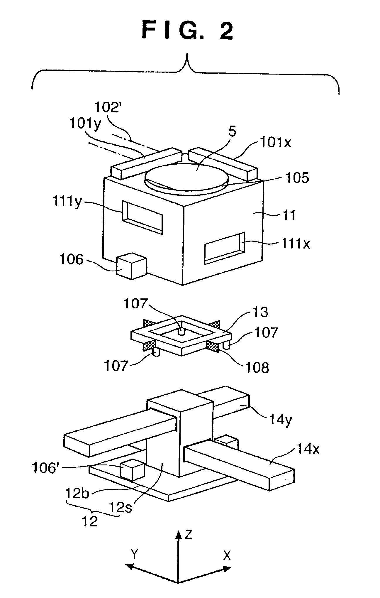
[0066]FIGS. 4A and 4B are views showing an electron beam exposure apparatus according to the third embodiment of the present invention. The Y-axis direction in this embodiment is a direction perpendicular to the array direction of a plurality of electron beams (B1, B2, B3, . . . ). As shown in FIG. 4A, the θ measurement 102′ is preferably performed in a direction perpendicular to the array direction of the plurality of beams. A tilt frame 13 is supported on a bottom plate 12b of a center slider 12 through Z actuators 107 for driving a θZ tilt stage 11 in the Z direction. The tilt frame 13 is arranged to surround the center slider 12. As the Z actuators 107, piezoelectric devices with guides which are rigid in the X-Y plane may be used. The θZ tilt stage 11 is supported on the tilt frame 13 through θ free leaf springs 108 serving as a connecting member with a degree of freedom in only the θ direction (rotation direction about the Z-axis). The θ free leaf springs 108 are arranged in the X-axis direction, and the others, in the Y-axis direction. The θZ tilt stage 11 is rigid with respect to the tilt frame 13 in the Z-axis direction. The θZ tilt stage 11 has a cage structure surrounding the center slider 12 and has apertures 111x and 111y, through which an X movable guide 14x and a Y movable guide 14y extend.
[0067]A θ linear motor movable element 106, which constitutes a part of an electromagnetic actuator, is fixed on the side surface of the θZ tilt stage 11. A θ linear motor stator 106′ which constitutes the remainder of the electromagnetic actuator is fixed on the bottom plate 12b to face the θ linear motor movable element 106. Since the θ linear motor movable element 106 and θ linear motor stator 106′ are in non-contact with each other, the substrate stage can be driven in a non-contact manner. It is thermally preferable that the θ linear motor movable element 106 comprises a magnet, and the θ linear motor stator 106′ comprises a coil. The θ linear motor movable element 106 and θ linear motor 106′ are preferably coated with multiple electromagnetic shields. For this reason, a magnet serving as the θ linear motor movable element 106 is preferably coated with multiple electromagnetic shields of, e.g., permalloy to avoid any variation in magnetic field. In addition, the magnet serving as the θ linear motor movable element 106 is preferably spaced apart from a reduction electron optical system 4 by a sufficient distance to avoid any variation in magnetic field due to a leakage magnetic field from the reduction electron optical system 4. More specifically, the θ linear motor movable element 106 and the substrate are desirably located on the opposite sides of the barycenter of the center slider 12 in the Z-axis direction. The θ linear motor stator 106′ may be arranged on the tilt frame 13.
[0068]Moreover, in this embodiment, the tilt frame 13 comprises electromagnets 130 as electromagnetic actuators which are actuated in only the Y-axis direction, as shown in FIG. 4B. This can reduce the load on the θ linear motor at the time of acceleration/deceleration in the Y-axis direction and the size of the θ linear motor (the θ linear motor movable element 106 and θ linear motor stator 106′). Each electromagnet 130 is preferably coated with multiple electromagnetic shields of, e.g., permalloy to avoid any variation in magnetic field. In addition, the electromagnet 130 is preferably spaced apart from the reduction electron optical system 4 by a sufficient distance to avoid any variation in magnetic field due to a leakage magnetic field from the reduction electron optical system 4.
[Other Embodiment]
[0069]The manufacturing process of a semiconductor device using an electron beam exposure apparatus according to a preferred embodiment of the present invention will be described next. FIG. 8 shows the flow of the whole manufacturing process of the semiconductor device. In step 1 (circuit design), a semiconductor device circuit is designed. In step 2 (mask formation), a mask having the designed circuit pattern is formed. In step 3 (wafer manufacture), a wafer is manufactured by using a material such as silicon. In step 4 (wafer process), called a preprocess, an actual circuit is formed on the wafer by lithography using the prepared mask and wafer. Step 5 (assembly), called a post-process, is the step of forming a semiconductor chip by using the wafer formed in step 4, and includes an assembly process (chip encapsulation). In step 6 (inspection), the semiconductor device manufactured in step 5 undergoes inspections such as an operation confirmation test and a durability test. After these steps, the semiconductor device is completed and shipped (step 7).
[0070]FIG. 9 shows the detailed flow of the above-mentioned wafer process. In step 11 (oxidation), the wafer surface is oxidized. In step 12 (CVD), an insulating film is formed on the wafer surface. In step 13 (electrode formation), an electrode is formed on the wafer by vapor deposition. In step 14 (ion implantation), ions are implanted in the wafer. In step 15 (resist processing), a photosensitive agent is applied to the wafer. In step 16 (exposure), the circuit pattern is transferred onto the wafer using the above-mentioned electron beam exposure apparatus. In step 17 (development), the exposed wafer is developed. In step 18 (etching), the resist is etched except for the developed resist image. In step 19 (resist removal), an unnecessary resist after etching is removed. These steps are repeated to form multiple circuit patterns on the wafer.
[0071]As has been described above, the present invention can provide an electron beam exposure apparatus capable of, e.g., reducing a degradation in drawing accuracy and performing high-accuracy exposure.
[0072]As many apparently widely different embodiments of the present invention can be made without departing from the spirit and scope thereof, it is to be understood that the invention is not limited to the specific embodiments thereof except as defined in the appended claims.

PUM

no PUM

Description & Claims & Application Information

We can also present the details of the Description, Claims and Application information to help users get a comprehensive understanding of the technical details of the patent, such as background art, summary of invention, brief description of drawings, description of embodiments, and other original content. On the other hand, users can also determine the specific scope of protection of the technology through the list of claims; as well as understand the changes in the life cycle of the technology with the presentation of the patent timeline. Login to view more.

Similar technology patents

Projection display apparatus

InactiveUS20090161073A1Wide color reproduction rangeReduce degradationProjectorsOptical pathLiquid-crystal display
Owner:JVC KENWOOD CORP A CORP OF JAPAN

Classification and recommendation of technical efficacy words

  • Reduce degradation
  • High exposure

Anti-virus therapy for respiratory diseases

ActiveUS20070134763A1PrevalenceHigh exposureRespiratorsOrganic active ingredientsAnti virusAsthma
Owner:UNIV OF SOUTHAMPTON
Why Eureka
Try Eureka