Variable electronic shutter in CMOS imager with improved anti smearing techniques

Active Publication Date: 2005-08-23
CALIFORNIA INSTTE OF TECH
View PDF3 Cites 23 Cited by
  • Summary
  • Abstract
  • Description
  • Claims
  • Application Information

AI Technical Summary

Benefits of technology

[0008]In an embodiment, optical and diffusion shields for the in pixel storage part are provided. These shields may prevent leakage of charge from other areas into the in pixel storage part.
[0009]In addition, the effective photodiode and storage capacitance may be optimized in order to improve signal swing and lower the noise. The optimization may be carried out according to a ratio of optimum relationships between device capacitances. The disclosed pixel architecture may allow the in pixel capacitor to be implemented with a minimal impact on the f

Problems solved by technology

Many of these imagers may suffer from

Method used


Image

  • Variable electronic shutter in CMOS imager with improved anti smearing techniques
  • Variable electronic shutter in CMOS imager with improved anti smearing techniques
  • Variable electronic shutter in CMOS imager with improved anti smearing techniques

Examples


Embodiment Construction

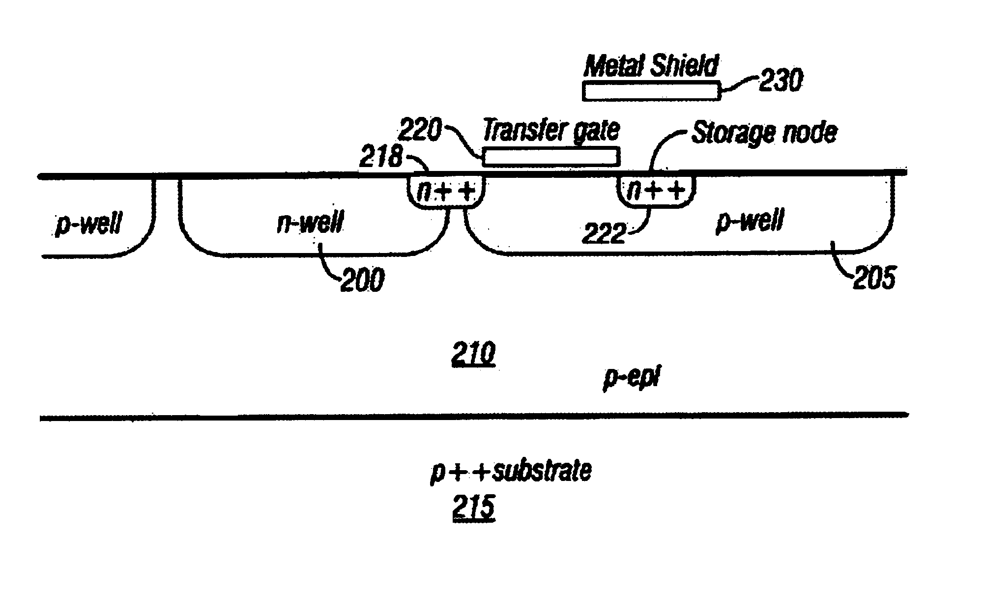
[0016]Imaging sensors with in pixel memories are known. However, the present inventors realize that the interframe smear and motion artifact may be due, at least partly, to seepage of charge from other areas, into the in-pixel memory. The charge may include charge that is left over from other exposure times, for example.

[0017]For example, if there is a 5 percent leakage into the memory part of the chip, there is a 20:1 ratio between frame readout time and exposure time. This may result in a 50 percent unwanted signal. This can correspondingly cause image smear. To the extent that the unwanted signal is representative of other exposure times, it may also introduce motion artifact.

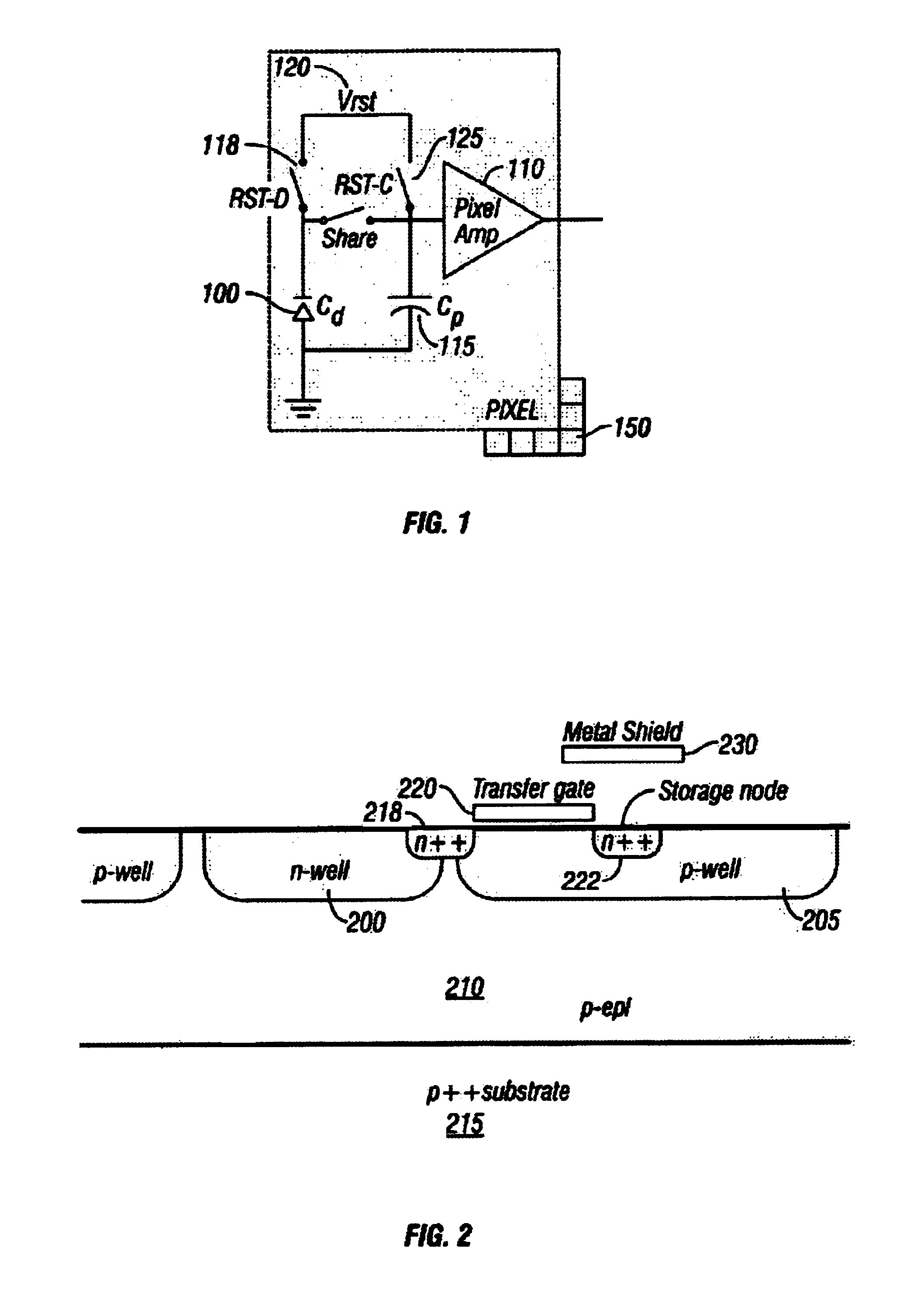
[0018]A snapshot imager is shown in FIG. 1. The basic embodiment includes an array of photoreceptors. A single photoreceptor 100 is shown, with the rest of the array being shown generically as 150.

[0019]Photoreceptor 100 is shown in a circuit with a pixel amplifier 110. In the embodiment, the photoreceptor 1...


PUM


Abstract

A leakage compensated snapshot imager provides a number of different aspects to prevent smear and other problems in a snapshot imager. The area where the imager is formed may be biased in a way that prevents photo carriers including electrons and holes from reaching a storage area. In addition, a number of different aspects may improve the efficiency. The capacitance per unit area of the storage area may be one, two or more orders of magnitude greater than the capacitance per-unit area of the photodiode. In addition, a ratio between photodiode capacitance and storage area capacitance is maintained larger than 0.7.

Description

CROSS REFERENCE TO RELATED APPLICATIONS[0001]This application claims priority from application Ser. No. 60 / 210,295, filed Jun. 8, 2000.[0002]U.S. Government may have certain rights in this invention pursuant to Nasa contract number NAS7-1407.BACKGROUND OF INVENTION[0003]Electronically shuttered imagers have been implemented using various image sensor technologies. For example, interline transfer charge coupled devices, CMOS active pixels, and pinned photodiode active pixels have been used for forming electronically shuttered imagers.[0004]Many of these imagers may suffer from interframe smear and motion artifacts.[0005]In addition, it may be desirable to provide the ability to program exposure time of such a device. The programmability may be programmable down to a level of a fraction of the frame readout time. This may operate to faithfully reproduce fast motion such as in sports photography.SUMMARY OF INVENTION[0006]The present application teaches a CMOS photodiode imager that pro...

Claims


Application Information

Patent Timeline
IPC IPC(8): H04N3/15H04N5/359
CPCH01L27/14623H04N5/359H04N25/62
Inventor PAIN, BEDABRATA
Owner CALIFORNIA INSTTE OF TECH
Why Eureka
Try Eureka