Light emitting device and method of manufacturing the same

a technology of light emitting devices and manufacturing methods, applied in the field of display panels, can solve the problems of increased consumption power, deterioration of tft characteristics, failure of tft operation, etc., and achieve the effect of low consumption power

Inactive Publication Date: 2005-08-23
SEMICON ENERGY LAB CO LTD
View PDF76 Cites 96 Cited by
  • Summary
  • Abstract
  • Description
  • Claims
  • Application Information

AI Technical Summary

Benefits of technology

[0011]Thus, an object of the present invention is to provide a structure of a light emitting device in which low consumption power is realized even in the case of a large screen and a method of manufacturing the same.
[0012]The present invention is intended to plate a surface of a source signal line or a surface of a power supply line in a pixel portion and thus to reduce the resistance of a wiring. Note that, in the present invention, the source signal line in the pixel portion is manufactured by a process different form a process of manufacturing a source signal line in a driver circuit portion. Also, the power supply line in the pixel portion is manufactured by a process different form a process of manufacturing a power supply line led onto a substrate. Further, with respect to a terminal, the same plating is performed to reduce the resistance.

Problems solved by technology

Therefore, a failure in the operation of the TFT and a deterioration of a TFT characteristic are caused.
Thus, a problem such as an increase of consumption power is caused.
Therefore, particularly, in the case of a panel with 3 inches or more, due to the influence of the wiring resistance, intensities in both ends of the screen are different from each other or crosstalk is caused.

Method used


Image

  • Light emitting device and method of manufacturing the same
  • Light emitting device and method of manufacturing the same
  • Light emitting device and method of manufacturing the same

Examples


embodiment 1

(Embodiment 1)

[0091]In this embodiment, a method of simultaneously manufacturing TFTs composing a pixel portion and TFTs composing a driver circuit provided in the vicinity of the pixel portion (CMOS circuit composed of an n-channel TFT and a p-channel TFT) on the same substrate will be described with reference to FIGS. 3A to 3c to FIG. 6.

[0092]First, in this embodiment, a substrate 200 made of glass such as barium borosilicate glass (represented by #7059 glass, #1737 glass, or the like, which is produced by Corning Corporation) or aluminoborosilicate glass is used. The substrate 200 is not particularly limited if it has translucency, and a quartz substrate may be used. Also, a plastic substrate having a heat resistance resistant to a processing temperature in this embodiment may be used.

[0093]Next, a base film 201 made from an insulating film such as a silicon oxide film a silicon nitride film, or a silicon oxynitride film is formed on the substrate 200. In this embodiment, a two l...

embodiment 2

(Embodiment 2)

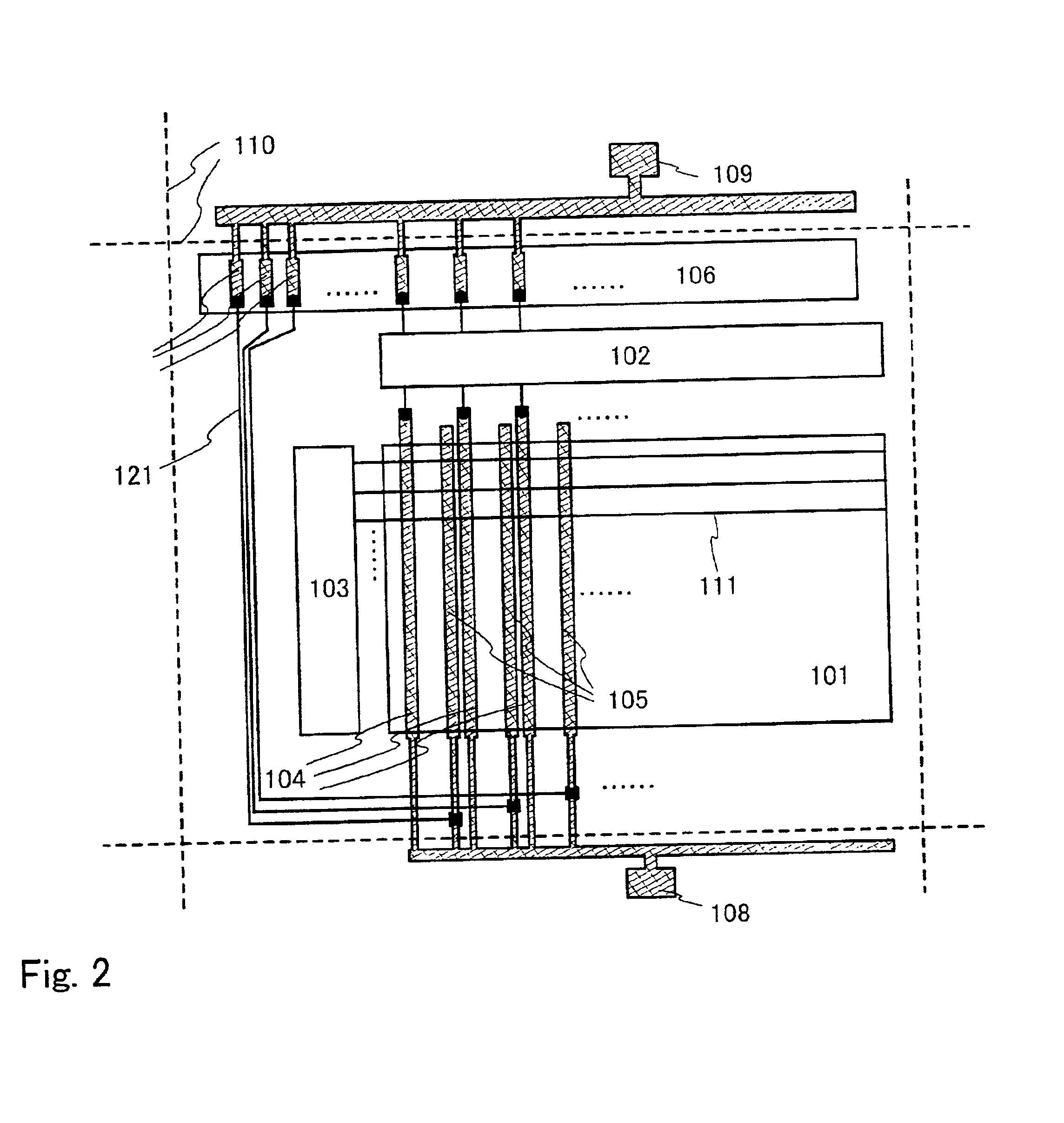
[0151]In Embodiment 1, the example in which the CMOS circuit is formed in the driver circuit is indicated. However, an NMOS circuit may be formed using only n-channel TFTs. Note that, when the NMOS circuit is formed by a combination of the n-channel TFTs, there are the case where it is formed using only enhancement TFTs as shown in FIG. 11A (hereinafter referred to as an EEMOS circuit) and the case where it is formed by a combination of an enhancement TFT and a depletion TFT as shown in FIG. 11B (hereinafter referred to as an EDMOS circuit). Also, TFTs provided in the pixel portion may be formed using only the n-channel TFTs. Note that the pixel electrode is preferably a cathode in this case. FIG. 10 is a cross sectional view of a light emitting device of this embodiment. Note that a state after a pixel electrode 547 is formed and before a third interlayer insulating film is formed is shown in FIG. 10.

[0152]Reference numeral 501 denotes a driver circuit including TFTs ...

embodiment 3

(Embodiment 3)

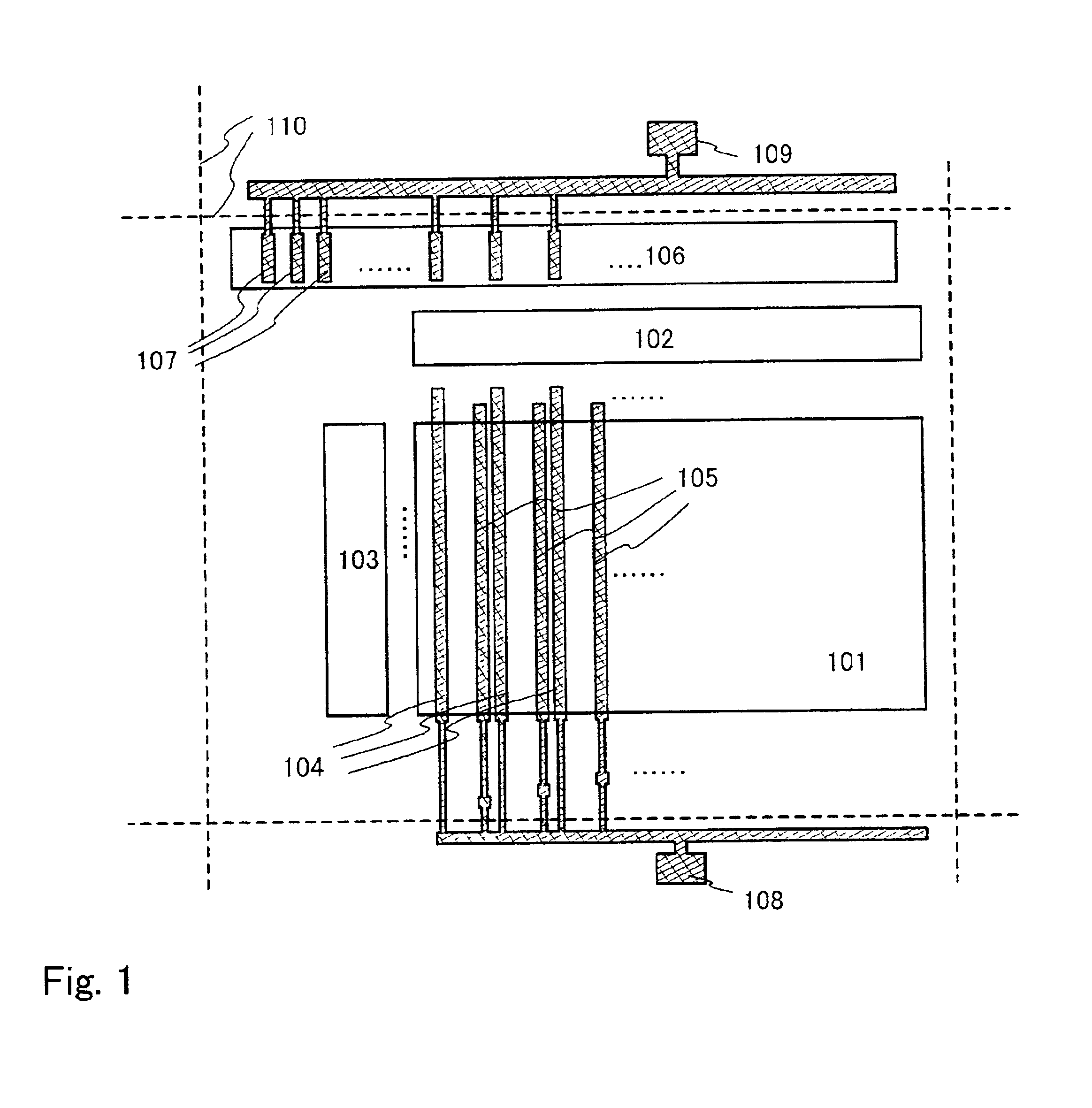
[0162]In this embodiment, a dummy pattern in the case where a source signal line included in a pixel portion, a power supply line included in the pixel portion and a terminal are connected with the same plating electrode and electroplating is performed will be described.

[0163]FIG. 13 is a top surface view of a light emitting device of this embodiment. Note that three source signal lines 604 in the pixel portion and three power supply lines 605 are typically shown in FIG. 13. The source signal lines 604 in the pixel portion are in parallel with one another and have a belt shape. The power supply lines 605 in the pixel portion are in parallel with one another and have a belt shape. Six terminals 607 are typically shown.

[0164]Reference numeral 601 denotes a pixel portion. The source signal lines 604 before plating and the power supply lines 605 before plating are provided in the pixel portion 601. The plurality of (six) terminals 607 before plating are formed in a termina...


PUM


Abstract

There is provided a light emitting device in which low power consumption can be realized even in the case of a large screen. The surface of a source signal line or a power supply line in a pixel portion is plated to reduce a resistance of a wiring. The source signal line in the pixel portion is manufactured by a step different from a source signal line in a driver circuit portion. The power supply line in the pixel portion is manufactured by a step different from a power supply line led on a substrate. A terminal is similarly plated to made the resistance reduction. It is desirable that a wiring before plating is made of the same material as a gate electrode and the surface of the wiring is plated to form the source signal line or the power supply line.

Description

BACKGROUND OF THE INVENTION[0001]1. Field of the Invention[0002]The present invention relates to a display panel in which a light emitting element formed on a substrate is sealed between the substrate and a cover member. Also, the present invention relates to a display module in which an IC is mounted in the display panel. Note that, in this specification, the display panel and the display module are generically called a light emitting device. Further, the present invention relates to electronic equipment using the light emitting device.[0003]2. Description of the Related Art[0004]Since a light emitting element itself emits light, visibility is high, a back light required for a liquid crystal display device (LCD) is unnecessary, it is suitable for thinness, and there is no limitation for a view angle. Thus, recently, a light emitting device using a light emitting element is noted as a display device alternative to a CRT and an LCD.[0005]The light emitting element has a layer includi...

Claims


Application Information

Patent Timeline
Patent Type & Authority Patents(United States)
IPC IPC(8): H01L27/32H01L27/28H05B33/04H01L51/56
CPCH01L27/3276H01L27/3279H01L27/3223H01L27/3246H01L51/56H01L2924/0002H01L2227/323H01L2924/00H10K59/88H10K59/1315H10K59/122H10K59/131H10K59/1201H10K71/00H10K59/10H01L27/1214
Inventor YAMAZAKI, SHUNPEIKOYAMA, JUNOSADA, MAI
Owner SEMICON ENERGY LAB CO LTD
Why Eureka
Try Eureka