Integrated circuit die having a copper contact and method therefor

a technology of integrated circuits and copper contacts, which is applied in the direction of electrical equipment, semiconductor devices, semiconductor/solid-state device details, etc., can solve the problems of increasing processing costs, increasing processing costs, and unable to achieve wire bonding directly to copper using existing production assembly equipments

Inactive Publication Date: 2005-08-23
APPLE INC
View PDF16 Cites 32 Cited by
  • Summary
  • Abstract
  • Description
  • Claims
  • Application Information

AI Technical Summary

Problems solved by technology

However, wire bonding directly to copper is not feasible using existing production assembly equipments due to the instability of the native copper oxide at wire bonding temperatures (typically greater than 130 degrees to 170 degrees Celsius).
However, adding an aluminum capping layer increases processing costs.
Furthermore, the use of an aluminum capping layer also requires the use of a barrier layer and/or a glue layer ...

Method used


Image

  • Integrated circuit die having a copper contact and method therefor
  • Integrated circuit die having a copper contact and method therefor
  • Integrated circuit die having a copper contact and method therefor

Examples


Embodiment Construction

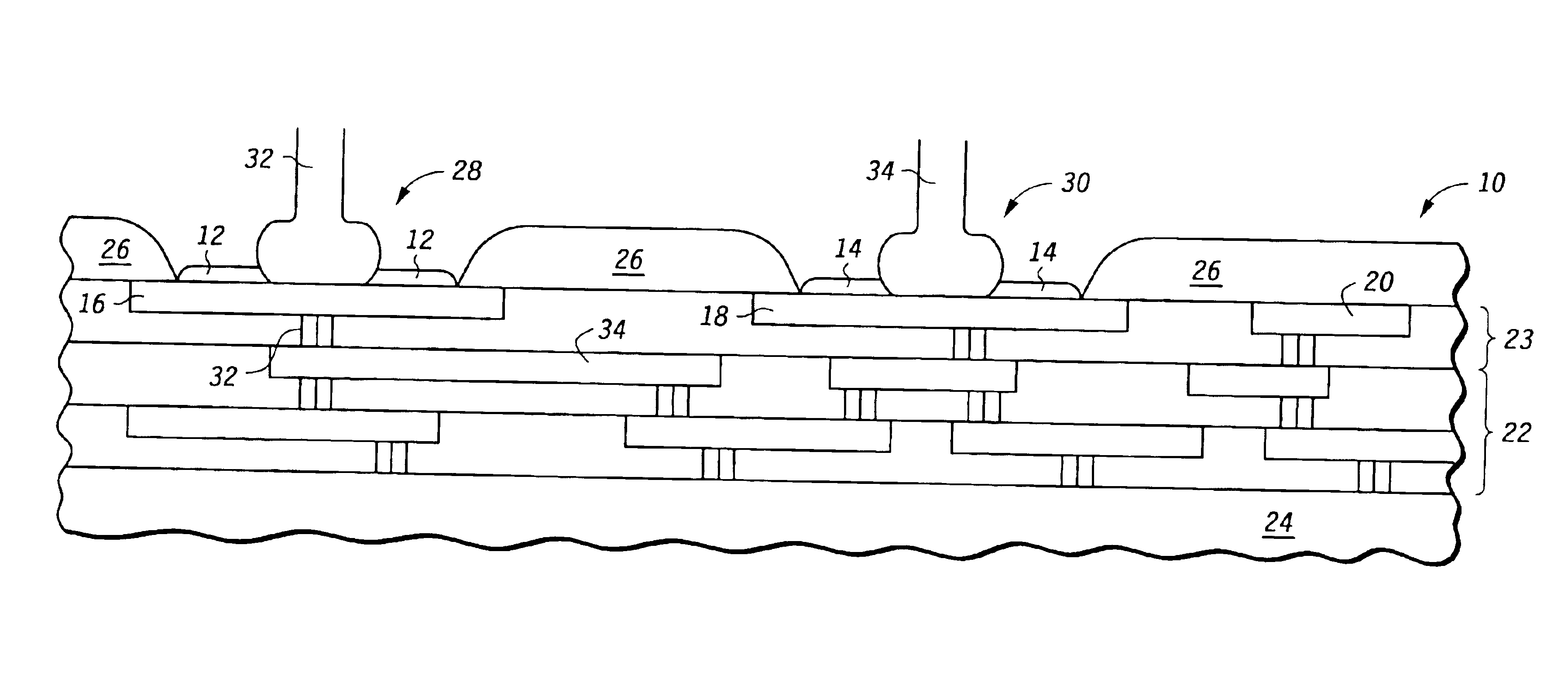
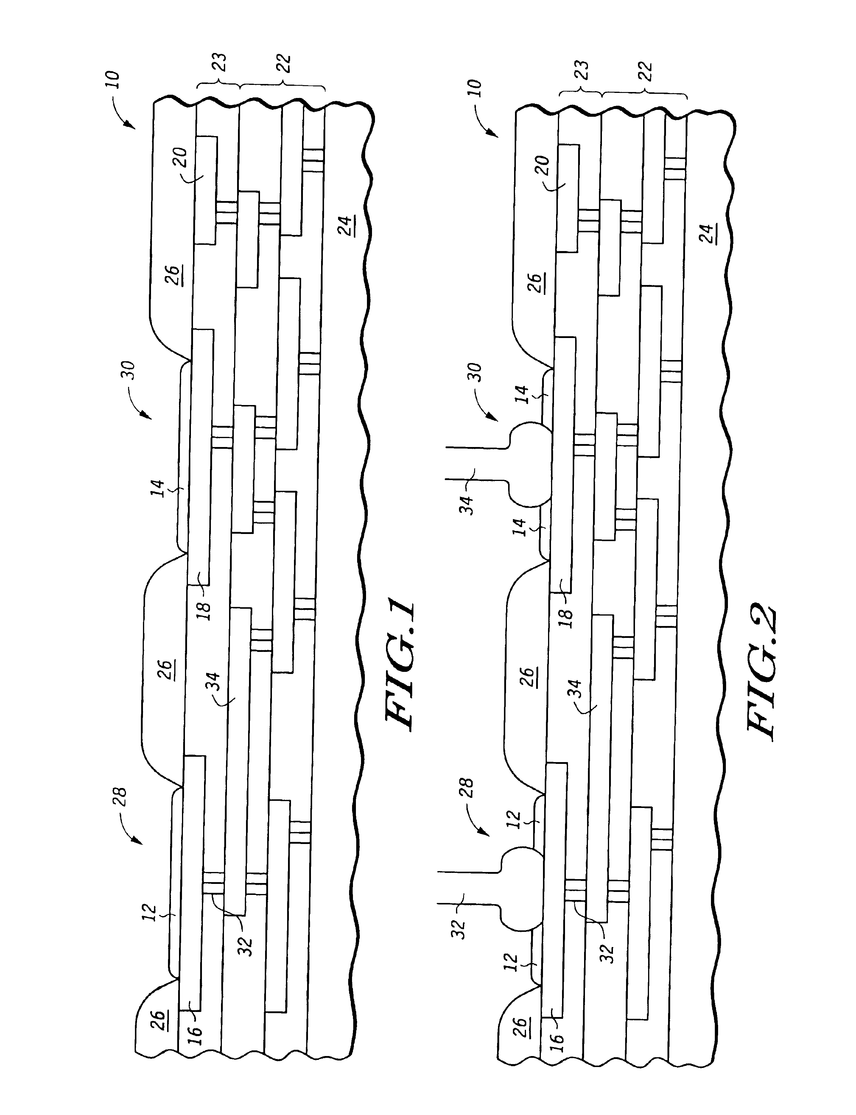
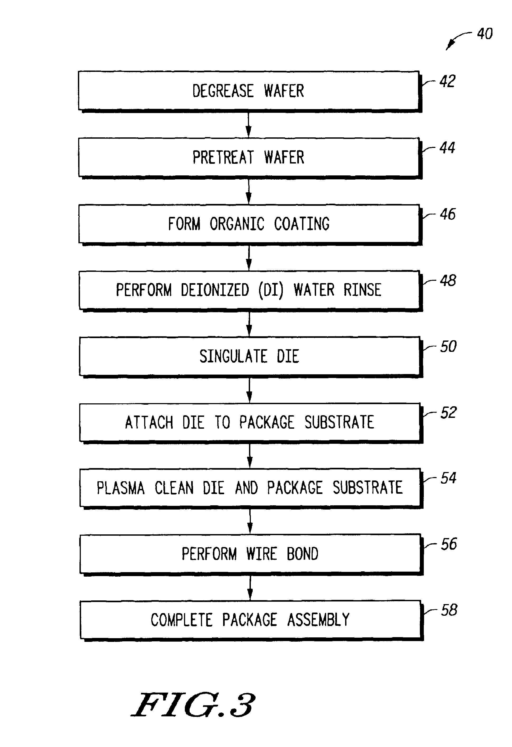
[0011]Generally, embodiments of the present invention provide an integrated circuit die having copper contacts coated with an organic material. The organic coating helps to prevent or limit copper oxidation of exposed copper contacts which can become especially problematic at temperatures greater than room temperature and even more problematic at temperatures greater than 100 degrees Celsius. For example, in a wire bonding process, the organic coating can be used to prevent excessive copper oxidation such that an improved wire bond can be formed to the copper contact. The organic coating may also be used in a variety of other applications to prevent or limit copper oxidation to achieve improved reliability and thermal resistance.

[0012]FIG. 1 illustrates a portion of an integrated circuit die 10 having active circuitry 24, metal interconnect layers 22 overlying active circuitry 24, final metal interconnect layer 23 overlying metal interconnect layers 22, and passivation layer 26 over...


PUM


Abstract

An integrated circuit die (10) has a copper contact (16, 18), which, upon exposure to the ambient air, forms a native copper oxide. An organic material is applied to the copper contact which reacts with the native copper oxide to form an organic coating (12, 14) on the copper contact in order to prevent further copper oxidation. In this manner, further processing at higher temperatures, such as those greater than 100 degrees Celsius, is not inhibited by excessive copper oxidation. For example, due to the organic coating, the high temperature of the wire bond process does not result in excessive oxidation which would prevent reliable wire bonding. Thus, the formation of the organic coating allows for a reliable and thermal resistance wire bond (32, 34). Alternatively, the organic coating can be formed over exposed copper at any time during the formation of the integrated circuit die to prevent or limit the formation of copper oxidation.

Description

FIELD OF THE INVENTION[0001]The present invention relates generally to integrated circuits, and more particularly, to integrated circuit die having copper contacts.BACKGROUND OF THE INVENTION[0002]In integrated circuit manufacturing, wire bonding is a well proven method used to connect a semiconductor die having electrical circuitry to a pin on a component package. It is also becoming increasingly common to use copper metal interconnects. However, wire bonding directly to copper is not feasible using existing production assembly equipments due to the instability of the native copper oxide at wire bonding temperatures (typically greater than 130 degrees to 170 degrees Celsius).[0003]One solution available today is the use of an aluminum capping layer which is used over the copper bond pads such that the wire bonds are bonding to the aluminum rather than the copper. However, adding an aluminum capping layer increases processing costs. Furthermore, the use of an aluminum capping layer ...

Claims


Application Information

Patent Timeline
IPC IPC(8): H01L23/485H01L23/48H01L21/60
CPCH01L24/03H01L24/05H01L24/48H01L24/85H01L24/45H01L2224/02166H01L2224/04042H01L2224/05647H01L2224/45124H01L2224/45144H01L2224/45147H01L2224/48463H01L2224/85013H01L2224/85375H01L2924/01002H01L2924/01005H01L2924/01006H01L2924/01007H01L2924/01011H01L2924/01013H01L2924/01018H01L2924/01028H01L2924/01029H01L2924/01033H01L2924/01039H01L2924/01079H01L2924/01082H01L2924/14H01L2924/19042H01L2924/30107H01L2924/00014H01L2924/01019H01L2224/78H01L2224/48747H01L2924/00H01L2224/48647H01L2224/48847H01L2924/12042H01L2224/85207H01L2224/8592
Inventor LEE, CHU-CHUNGHARUN, FUAIDAHESS, KEVIN J.TAN, LAN CHUYONG, CHENG CHOI
Owner APPLE INC
Why Eureka
Try Eureka