Precoding circuit and precoding-mulitplexing circuit for realizing very high transmission rate in optical fiber communication

a transmission rate and optical fiber technology, applied in pulse technique, instruments, baseband system details, etc., can solve the problems of complexed signals that cannot be processed, the delay time required for the feedback to the exor circuit would become longer than one time-slot time, and the realization of one-bit delay is difficult. , to achieve the effect of handling very high transmission rate and simple configuration

Inactive Publication Date: 2005-08-23
NIPPON TELEGRAPH & TELEPHONE CORP
View PDF19 Cites 15 Cited by
  • Summary
  • Abstract
  • Description
  • Claims
  • Application Information

AI Technical Summary

Benefits of technology

[0028]It is therefore an object of the present invention to provide a precoding circuit and a pr...

Problems solved by technology

However, in the case where the conventional precoding circuit is used in processing multiplexed signals which have the same rate as the transmission rate as a result of the time division multiplexing of electric signals by the multiplexer as shown in FIG. 1, the following problems occur if an attempt to make the transmission rate even higher.
First, there is a problem in that the multiplexed signals cannot be processed because of the limitation on the bit rate of the EXOR circuit.
Second, there is a problem in that the realization of one-bit delay is difficult.
However, if the propagation delay of the circuit becomes unignorable compared with a time-slot of one bit duo to the increase of the transmission rate, the delay time required for the feedback to the EXOR circuit would become longer than one time-...

Method used


Image

  • Precoding circuit and precoding-mulitplexing circuit for realizing very high transmission rate in optical fiber communication
  • Precoding circuit and precoding-mulitplexing circuit for realizing very high transmission rate in optical fiber communication
  • Precoding circuit and precoding-mulitplexing circuit for realizing very high transmission rate in optical fiber communication

Examples


first embodiment

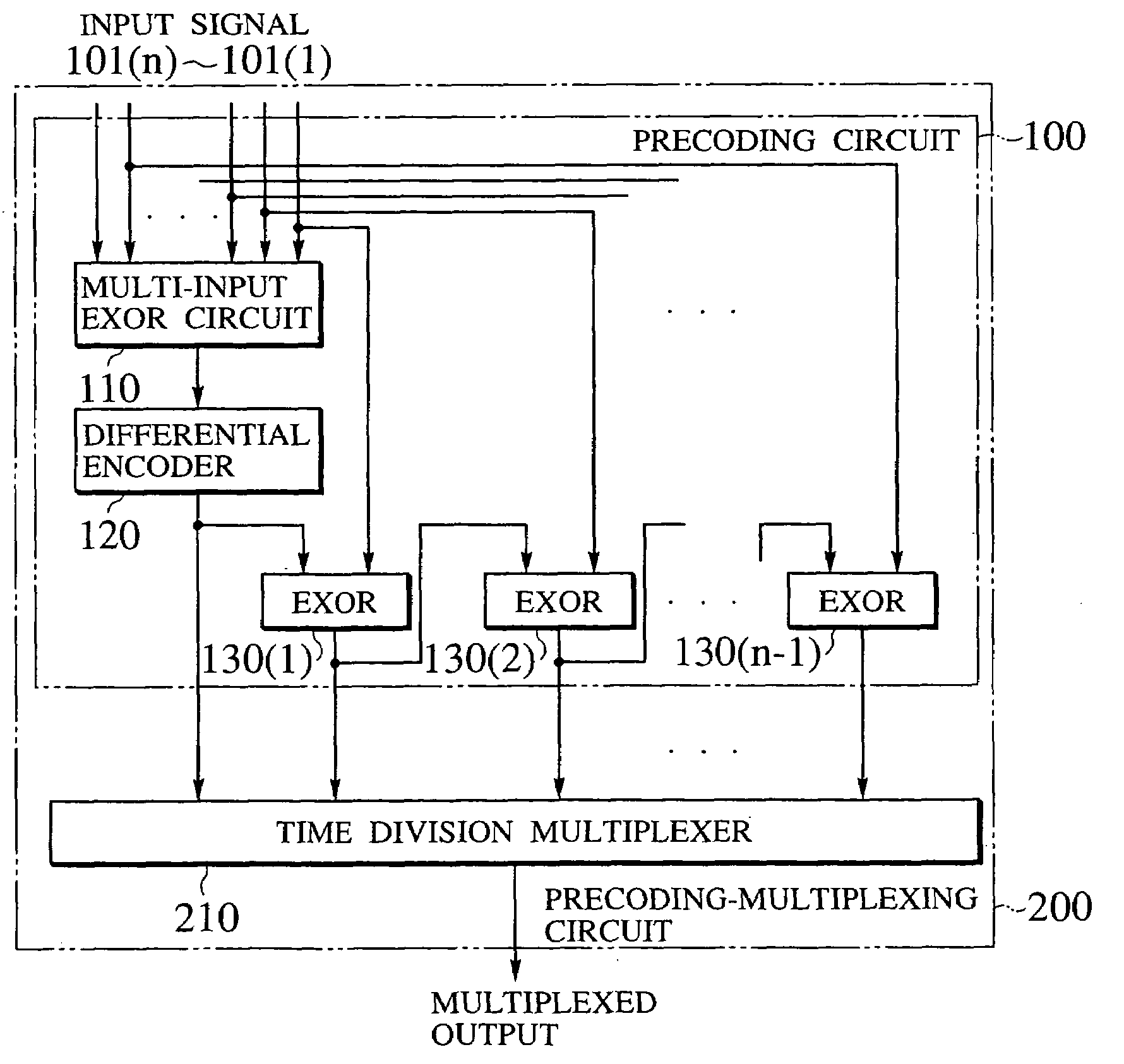
[0056]Referring now to FIG. 5 to FIG. 12, a precoding circuit and a precoding-multiplexing circuit according to the present invention will be described in detail.

[0057]FIG. 5 shows a schematic configuration of a precoding-multiplexing circuit in this first embodiment, and FIG. 6 shows a detailed configuration of the precoding-multiplexing circuit of FIG. 5. FIG. 7 shows one exemplary configuration of a multi-input EXOR circuit used in the configuration of FIG. 6, and FIG. 8 shows another exemplary configuration of a multi-input EXOR circuit used in the configuration of FIG. 6.

[0058]FIG. 9 shows a configuration of the precoding-multiplexing circuit of the first embodiment in an exemplary case of the number of multiplexing n=2, and FIG. 10 shows exemplary signals in the precoding-multiplexing circuit of FIG. 9. FIG. 11 shows a configuration of the precoding-multiplexing circuit of the first embodiment in an exemplary case of the number of multiplexing n=4, and FIG. 12 shows exemplary ...

second embodiment

[0098]Referring now to FIG. 13 and FIG. 14, a preceding circuit and a precoding-multiplexing circuit according to the present invention will be described in detail.

[0099]FIG. 13 shows a configuration of the precoding-multiplexing circuit of the second embodiment, and FIG. 14 shows exemplary signals in the precoding-multiplexing circuit of FIG. 13. Note that the delay time of the circuit elements other than half-bit delays 151, 155 and 156 of FIG. 13 is ignored in FIG. 14.

[0100]The input signals 101 to be entered into the precoding-multiplexing circuit 200C shown in FIG. 13 are two parallel binary signals in the bit rate that is ½ of the transmission rate. Namely, two signals before the time division multiplexing are entered as parallel input signals 101(1) and 101(2).

[0101]The precoding-multiplexing circuit 200C of FIG. 13 comprises a preceding circuit 100C and a selector 215. The selector 215 has the same function as the time division multiplexer 210 of the first embodiment.

[0102]A...

third embodiment

[0114]Referring now to FIG. 15 and FIG. 16, a precoding circuit according to the present invention will be described in detail.

[0115]FIG. 15 shows a configuration of the preceding circuit of the third embodiment, and FIG. 16 shows exemplary signals in the precoding circuit of FIG. 15.

[0116]The precoding circuit of FIG. 15 fulfills the same function as the conventional precoder of FIG. 1. However, the precoding circuit of FIG. 15 has a configuration which is devised to shorten the internal delay time.

[0117]In FIG. 15, a D-type flip-flop 160 connected to an output of an EXOR circuit 161 realizes the one bit time delay.

[0118]As shown in FIG. 16, there is a time lag of about one period of the clock signal between the input (EXOR output) and the output (output signal) of the D-type flip-flop 160. When the propagation delay of the circuit becomes unignorable compared with a time-slot of one bit due to the increase of the transmission rate, there is a possibility for a delay time required ...


PUM


Abstract

A precoding-multiplexing circuit is formed by a precoding circuit for carrying out a precoding with respect to n sets of parallel input binary data signals having a bit rate equal to R/n, to obtain n sets of parallel precoded signals, and a time division multiplexer for time division multiplexing the parallel precoded signals obtained by the precoding circuit, in units of one bit, and outputting time division multiplexed output signal having a bit rate equal to R. In this configuration, the encoding is realized by processing electric signals before the time division multiplexing, so that it becomes possible for the preceding circuit to handle signals which are slower than the transmission rate, and therefore it becomes easier to realize the higher transmission rate.

Description

BACKGROUND OF THE INVENTION[0001]1. Field of the Invention[0002]The present invention relates to a preceding circuit and a precoding-multiplexing circuit for use in generation of very high speed signals to be utilizing in an optical fiber communication system.[0003]2. Description of the Background Art[0004]In the very high speed optical fiber communication system, the influence of the chromatic dispersion of an optical fiber transmission line becomes noticeable.[0005]As a transmission scheme with a high dispersion tolerance, the optical duobinary transmission scheme is known. The optical duobinary transmission scheme can realize the dispersion tolerance approximately twice higher than that of the Non-Return-to-Zero (abbreviated hereafter as NRZ) transmission scheme, so that it is expected to be applicable to the very high speed optical transmission system (see K. Yonenaga and S. Kuwano, “Dispersion-Tolerant Optical Transmission System Using Duobinary Transmitter and Binary Receiver”...

Claims


Application Information

Patent Timeline
IPC IPC(8): H04L25/497H04J3/00H04J3/04H04J14/08H04L25/02
CPCH04L25/497
Inventor YONENAGA, KAZUSHIGEYONEYAMA, MIKIOMURATA, KOICHIMIYAMOTO, YUTAKA
Owner NIPPON TELEGRAPH & TELEPHONE CORP
Why Eureka
Try Eureka