
Reticle alignment procedure

a technology of reticle pattern and alignment procedure, which is applied in the field of wafer alignment methods, can solve the problems of reducing surface uniformity, distortion of am, and profound influence on circuit accuracy, and achieves the effect of removing bias resulting from precedent process and ensuring accuracy of reticle pattern transferring

Inactive Publication Date: 2005-08-30
UNITED MICROELECTRONICS CORP
View PDF1 Cites 0 Cited by
  • Summary
  • Abstract
  • Description
  • Claims
  • Application Information

AI Technical Summary

Benefits of technology

The present invention provides a method of aligning a semiconductor wafer using a reticle alignment machine (RAM) that prevents errors caused by previous layers. The method involves aligning a current-layer reticle with a pre-layer wafer alignment mark, capturing image signals of the reticle and the wafer, and calibrating the coordinates of the current layer to the wafer. This ensures accurate pattern transfer and prevents bias resulting from previous processes. The invention also includes a post-reticle alignment step using a VRA sensor and a charge couple device (CCD) camera to capture and compare image signals of the reticle and the wafer. Overall, the invention improves the accuracy and efficiency of the semiconductor manufacturing process.

Problems solved by technology

Circuit accuracy is profoundly affected by the AM, especially when process error happens.
However, when the AM is transferred from a precedent process onto the wafer, some inevitable process errors could occur, such as changes of temperature, time, and pressure that reduce the surface uniformity of wafer, or over polishing in the chemical mechanical polishing (CMP) process that cause the distortion of the AM.
Images and signals captured and transferred by the FIA, LSA, and LIA would be weakened or biased by inevitable process errors.
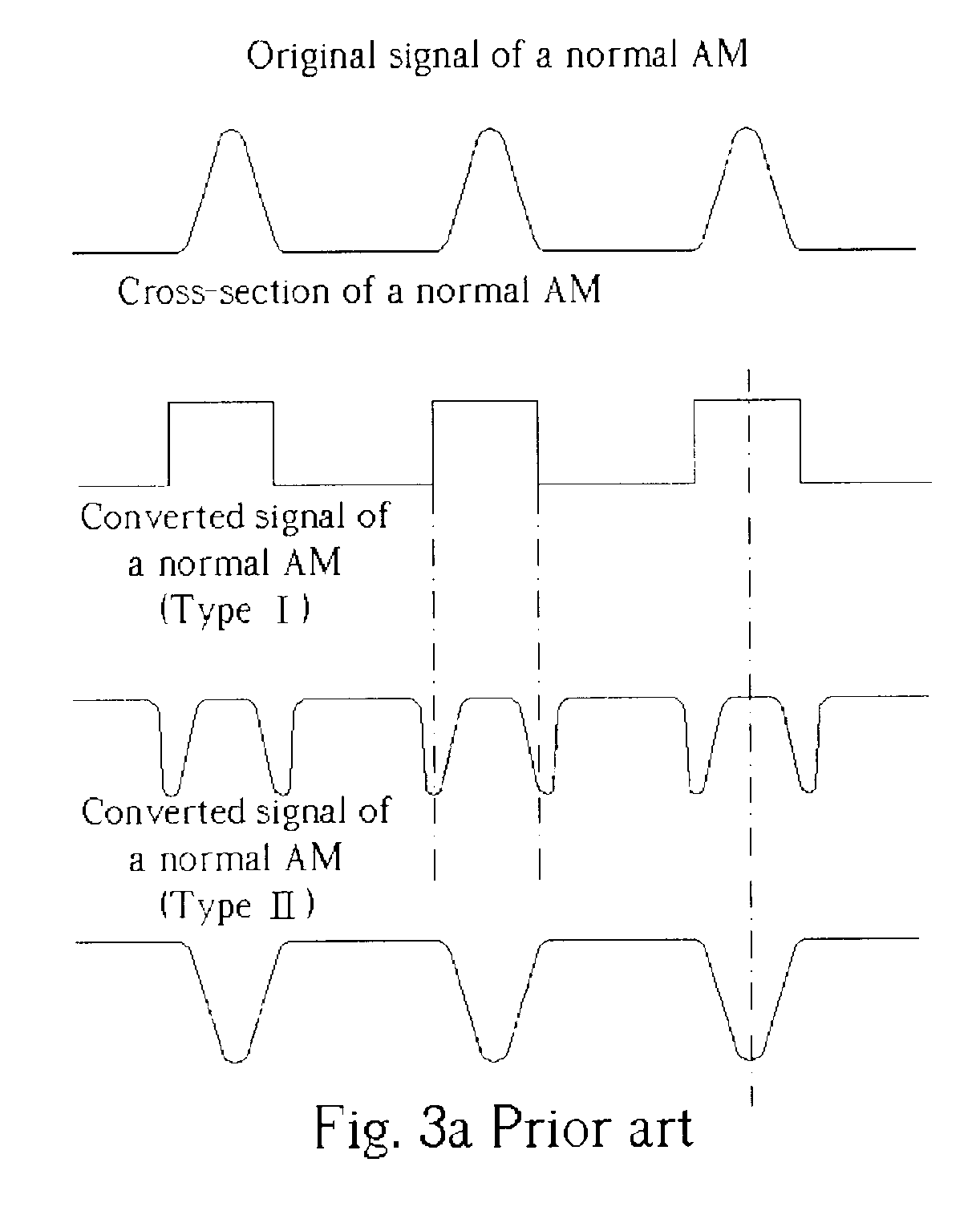
3(b), when the AM is damaged because of process errors, signals generated by the AM would derive unnecessary bias that is different from signals generated by a normal AM.

Method used


Image

  • Reticle alignment procedure
  • Reticle alignment procedure
  • Reticle alignment procedure

Examples


Embodiment Construction

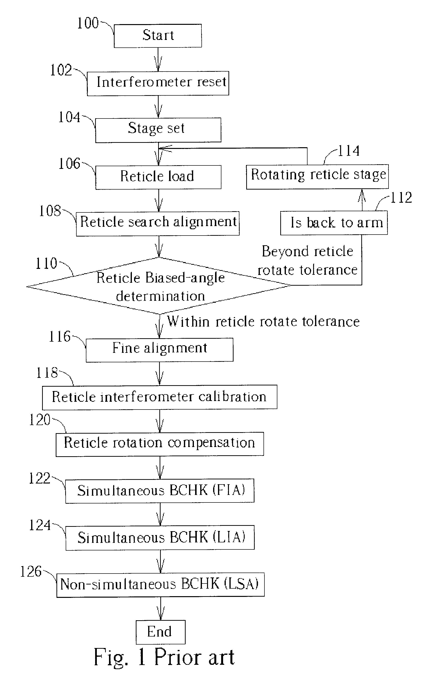
[0019]Please refer to FIG. 4. FIG. 4 is a flow chart of a reticle alignment procedure of the present invention. As shown in FIG. 4, the reticle alignment procedure of the present invention starts with a start step 400; a reticle having a current layer to be exposed is installed into an RAM. Then an interferometer reset step 402 is performed to reset an interferometer of the RAS, and a reticle stage set step 404 is performed with a field image alignment sensor (FIA sensor).

[0020]A reticle load step 406 is performed to load the reticle, and a reticle search alignment step 408 is performed with a video reticle alignment sensor (VRA sensor) to adjust the coordinates of the reticle by rotating the reticle. Then a reticle biased-angle determination step 410 is performed; if the reticle biased-angle is too large, the reticle is removed by a robot arm and rotated to reload, as step 412 and 414 show in FIG. 4. Afterward, a fine alignment step 416 is performed by utilizing a set of alignment ...


PUM

PropertyMeasurementUnit
areaaaaaaaaaaa
speedaaaaaaaaaa
charge couple device cameraaaaaaaaaaa

Abstract

A semiconductor wafer has at least one pre-layer on-wafer alignment mark (pre-layer on-wafer AM) on a top surface of the semiconductor wafer. A baseline check (BCHK) is performed to align a current-layer reticle AM on a current-layer reticle with the pre-layer on-wafer AM. By capturing and comparing signals of the current-layer reticle AM and the pre-layer on-wafer AM, a corresponding coordinate of the current-layer reticle to the semiconductor wafer is calibrated. Finally, a lithography process is performed to transfer the layout of the current-layer reticle AM to the top surface of the semiconductor wafer to form a corresponding current-layer on-wafer AM.

Description

BACKGROUND OF INVENTION[0001]1. Field of the Invention[0002]The present invention relates to a method of aligning wafers, and more particularly, to a method which utilizes a signal of an alignment mark captured from a reticle by a reticle alignment system (RAS) as standard signals to calibrate a pre-layer wafer alignment mark captured by a wafer alignment system (WAS), and further filters unnecessary bias resulting from process errors.[0003]2. Description of the Prior Art[0004]In the manufacturing process of integrated circuits (IC), the lithography process is one of the most important technologies. The quality of the lithography process is evaluated by critical dimension (CD) and alignment accuracy (AA). Besides the performance of the alignment system and the accuracy of metrology, the alignment mark (AM) on the wafer is another factor that affects the alignment accuracy. Circuit accuracy is profoundly affected by the AM, especially when process error happens. Therefore, to design ...

Claims


Application Information

Patent Timeline
Patent Type & Authority Patents(United States)
IPC IPC(8): G01B11/00G03F9/00G03C5/00G03F7/00H01L21/02H01L21/00H01L21/027
CPCG03F9/7011G03F9/7019G03F9/7088
Inventor YU, CHENG-HUNG
Owner UNITED MICROELECTRONICS CORP
Learn More