Programming and erasing methods for a non-volatile memory cell

a non-volatile, memory cell technology, applied in the direction of digital storage, instruments, transistors, etc., can solve the problems of cell failure to program verification, strategy not meeting the second requirement, wide variation of programming speed,

Inactive Publication Date: 2005-08-30
SPANSION ISRAEL
View PDF250 Cites 69 Cited by
  • Summary
  • Abstract
  • Description
  • Claims
  • Application Information

AI Technical Summary

Benefits of technology

[0047]An object of the present invention is to provide improved programming and erasure methods.

Problems solved by technology

If, however, during the read operation, the inversion layer is not strong enough to prevent the current flow through the channel, then the bit will be read as a “1”, and the cell will fail program verification.
However, this strategy will not meet the second requirement due to the many process and environmental parameters that affect the programming rate and its variations.
The wide variation of programming speeds creates problems during programming of memory cell arrays.
When an improper programming algorithm is used, some cells may receive too high programming voltages or may be programmed for too long.
1), creating reliability problems due to the degradation of the quality of the product.
Furthermore, continuing to apply high voltage pulses once the unit cells have already reached the programmed level wastes power and creates a power dissipation problem.
Moreover, as to be described below, in multi-level floating gate products, over-programming can lead to information read failures.
When a cell is over-programmed, the resultant threshold voltage may overshoot the desired region, thus leading to a read error or failure.
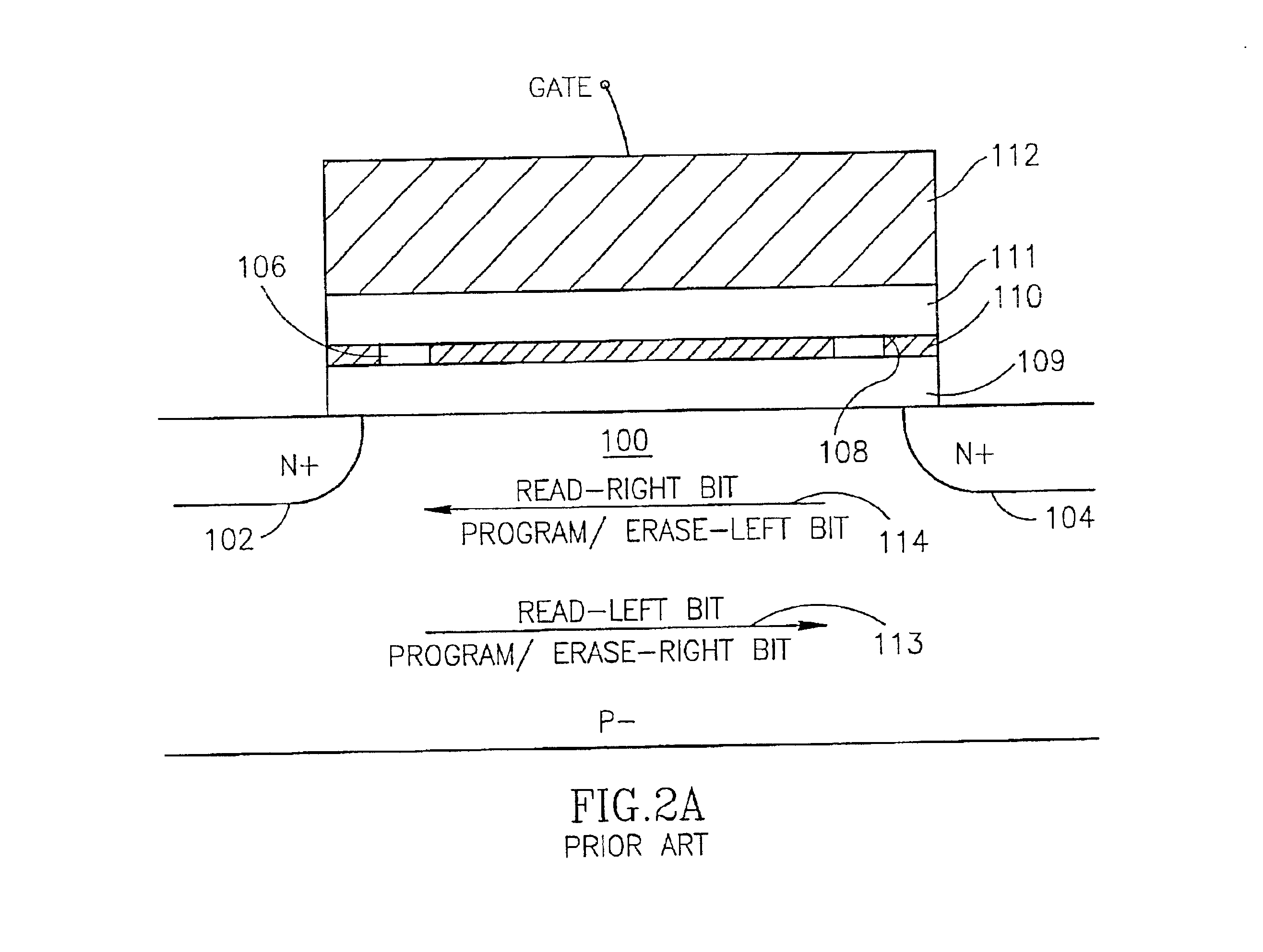
Further problems arise when programming both bits of multi-bit memory cells, such as the two-bit NROM cell.
In NROM cells, in addition to the stated problems connected with breakdown of the oxide layer and unnecessary dissipation of power, over-programming creates different problems.
As explained below in connection with FIGS. 6, over-programming results in quality deterioration and reliability degradation, as well as read failures in two-bit cells.
Applicants note that tail 44, which is farther from the bit line than the bulk of the trapped charge, is generally not removable during erasure and thus, reduces the ability of the NROM cell to withstand a large number of program and erase cycles.
Furthermore, the accumulation of trapped negative charge far from the junction increases the threshold voltage level, which affects the reverse read, making it difficult to distinguish the first bit from the second bit and creating read failures.
Unfortunately, prior art methods of gradually increasing the programming gate voltage VG are not effective for NROM cells, and tend to produce the following two problems:1. In NROM products, increases in the gate voltage VG do not linearly correlate to increases in the threshold voltage VTH, and the effect of the increases varies from cell to cell.
This causes a lack of precise programming control, and an incurred risk of over programming.2. In order to ensure a reasonable yield rate, meeting the programming rate requirement, the drain voltage VD potential must be high, creating trapped charge regions distant from the junction.
The above two problems result in reduction in the endurance of the product, increase in the charge loss and reduction in yield.
Reduction in the incremental increase of the gate voltage VG can alleviate part of the control problem, but it will dramatically increase the programming time.
Unfortunately, there are resultant difficulties at both ends of the dynamic range.
Low gate voltage VG results in cycling degradation.
Further increases in gate voltage VG, such as over 10V, require special processes and put severe limitations on the scaling of the ONO thickness due to charging by tunneling.
The second problem noted above (high drain voltage VD) creates even more severe limitations on the stepped gate voltage VG approach.
Accordingly, the resultant product is the undesirable tail 44, which drastically reduces the product's endurance.
Hence, due to the first problem noted above, using the gate voltage VG as a dynamic parameter for controlling programming is very limited in range.
In conclusion, in NROM cells, stepping the programming gate voltage VG does not provide tight programming control and is not effective in preventing over-programming and eventual degradation of the product's quality.
As can be understood from the above, when prior art programming algorithms are applied to the NROM cell, they do not sufficiently provide the abilities to produce increased programming speed while maintaining tight programming control.

Method used


Image

  • Programming and erasing methods for a non-volatile memory cell
  • Programming and erasing methods for a non-volatile memory cell
  • Programming and erasing methods for a non-volatile memory cell

Examples


Embodiment Construction

[0076]The present invention teaches an NROM cell algorithm which regulates the bit line voltage VBL provided to the bit line acting as the drain, thereby providing tight programming control. Furthermore, the described invention provides the combination of a fast programming algorithm with reduced over-programming risk, and hence improved product endurance and cycling ability.

[0077]Although a bit line can act as either a source or a drain, in the present application, references to the bit line voltage VBL refer to the voltage provided when the bit line is currently acting as a drain. For purposes of clarity herein, when the bit line acts as a source, it is herein referred to as a source.

[0078]The present invention further teaches the use of a low programming bit line voltage VBL to produce a tight spatial distribution of trapped charge, thereby resulting in better two-bit separation in the NROM cell, faster erase, and increased product life.

[0079]Furthermore, by controlling the bit l...


PUM


Abstract

A method for programming and erasing a memory array includes the step of adapting programming or erase pulses to the current state of the memory array. In one embodiment, the step of adapting includes the steps of determining the voltage level of the programming pulse used to program a fast bit of the memory array and setting an initial programming level of the memory array to a level in the general vicinity of the programming level of the fast bit. For erasure, the method includes the steps of determining erase conditions of the erase pulse used to erase a slowly erasing bit of said memory array and setting initial erase conditions of said memory array to the general vicinity of said erase conditions of said slowly erasing bit. In another embodiment of the array, the step of adapting includes the steps of measuring the current threshold level of a bit to within a given range and selecting an incremental voltage level of a next programming or erase pulse for the bit in accordance with the measured current threshold level.

Description

CROSS REFERENCE TO RELATED APPLICATIONS[0001]The present application is a divisional application of U.S. Ser. No. 09 / 730,586, filed Dec. 7, 2000, which application is a continuation in part application of Ser. No. 09 / 563,923, filed May 4, 2000 now U.S. Pat. No. 6,396,741, which application is incorporated herein by reference.FIELD OF THE INVENTION[0002]The present invention relates generally to electrically erasable, programmable read only memory (EEPROM) cells and specifically, to methods for programming thereof.BACKGROUND OF THE INVENTION[0003]FIG. 1, to which reference is made, illustrates a typical prior art floating gate cell, comprising two diffusion areas, source 102 and drain 104, embedded in a substrate 105, between which is a channel 100. A floating gate 101 is located above but insulated from channel 100, and a gate 112 is located above but insulated from floating gate 101.[0004]Typically, when programming the floating gate cell, programming voltages VG and VD are applied...

Claims


Application Information

Patent Timeline
Patent Type & Authority Patents(United States)
IPC IPC(8): G11C11/56G11C16/34G11C16/10G11C16/06G11C16/14G11C16/28G11C16/02G11C16/04H01L21/8247H01L27/115H01L29/788H01L29/792
CPCG11C11/5671G11C16/0475G11C16/10G11C16/14G11C16/3468G11C16/3481G11C16/28
Inventor AVNI, DROREITAN, BOAZ
Owner SPANSION ISRAEL
Why Eureka
Try Eureka