Contact assemblies, methods for making contact assemblies, and plating machines with contact assemblies for plating microelectronic workpieces
What is Al technical title?
Al technical title is built by PatSnap Al team. It summarizes the technical point description of the patent document.
a technology of contact assemblies and microelectronic workpieces, which is applied in the direction of machining electrodes, electrical-based machining electrodes, manufacturing tools, etc., to achieve the effect of reducing the electrical connection between the contact and the seed layer, and reducing the efficiency of the electrical connection
Inactive Publication Date: 2005-09-06
SEMITOOL INC
View PDF6 Cites 6 Cited by
Summary
Abstract
Description
Claims
Application Information
AI Technical Summary
This helps you quickly interpret patents by identifying the three key elements:
Problems solved by technology
Method used
Benefits of technology
[0010]The contact system can be coupled to the posts of the support member. The contact system can have a plurality of contact members projecting inwardly into the opening relative to the support member and transversely with respect to the access path. The contact members can comprise electrically conductive biasing elements, such as fingers, that have a contact site and a dielectric coating configured to expose the contact sites. In one embodiment
Problems solved by technology
Oxides are generally resistive, and thus oxides reduce the efficacy of the electrical connection between the contacts and the seed-layer.
Galvanic etching removes the seed-layer at the interface of the contacts, which can cause a non-uniform current distribution around
Method used
Image
Click on the blue label to locate the original text in one second.
Reading with bidirectional positioning of images and text.
Examples
Embodiment Construction
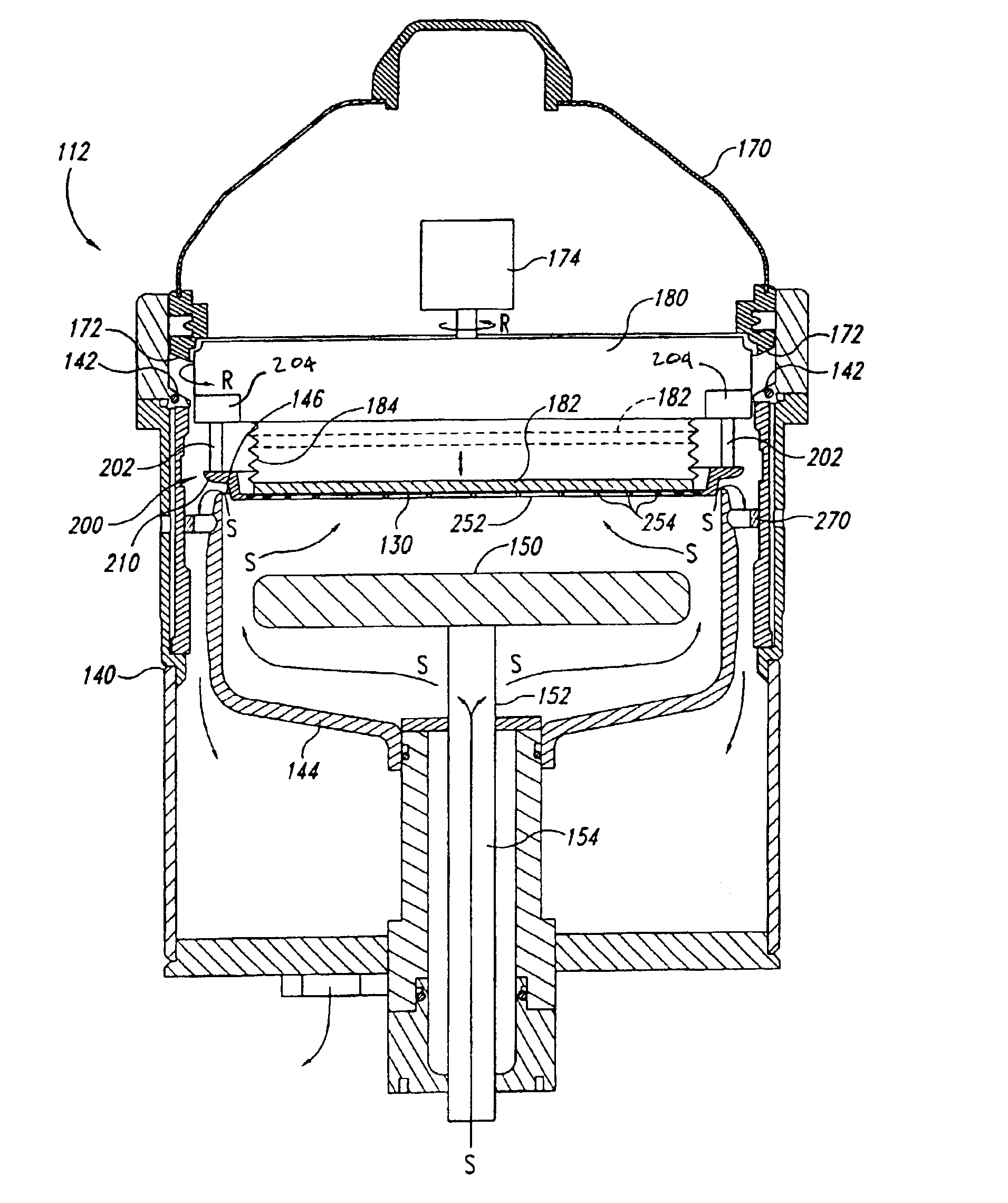
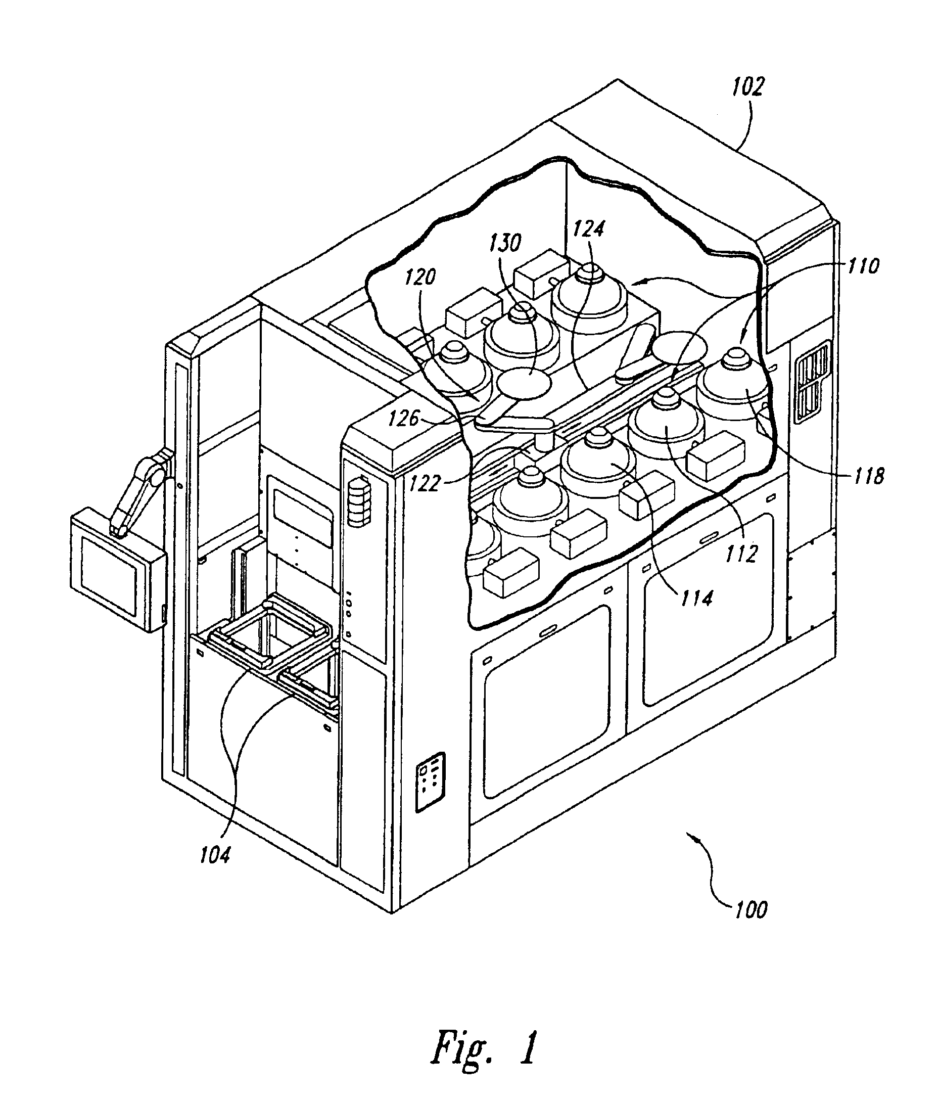
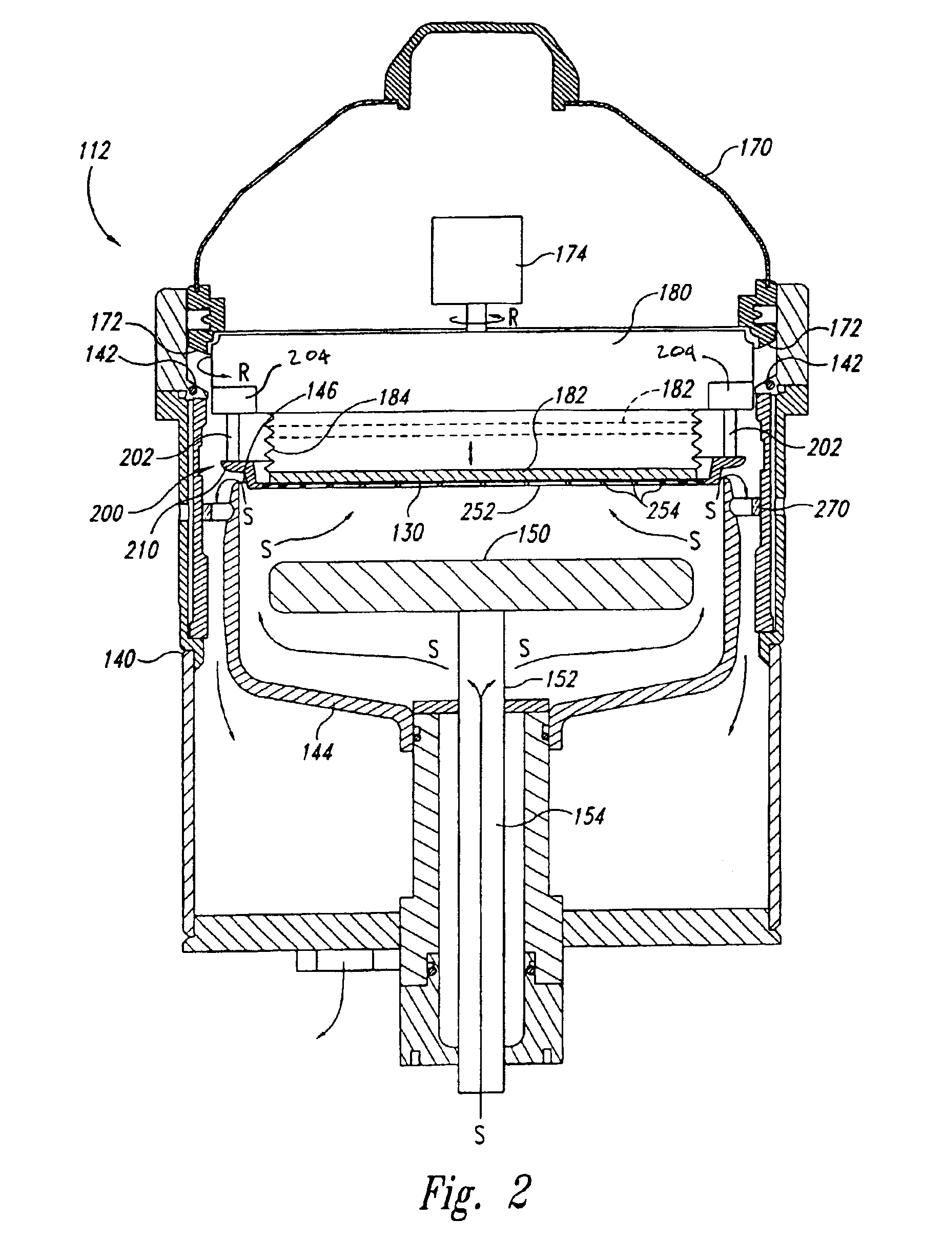
[0022]The following description discloses the details and features of several embodiments of contact assemblies, methods for making contact assemblies, and electroplating machines with contact assemblies for electroplating metal layers onto microelectronic workpieces. It will be appreciated that several of the details set forth below are provided to describe the foregoing embodiments in a manner sufficient to enable a person skilled in the art to make and use contact assemblies and electroplating systems in accordance with embodiments of the invention. Several of the details and advantages described below, however, may not be necessary to practice embodiments of the invention accordance with the following claims. For example, many of the embodiments described below are directed toward wet-contact assemblies, but these same devices can also be used in dry-contact assemblies as shown in PCT Application No. PCT / US99 / 15847. Additionally, the invention can also include additional embodim...
PUM
Property
Measurement
Unit
Angle
aaaaa
aaaaa
Radius
aaaaa
aaaaa
Electrical conductor
aaaaa
aaaaa
Abstract
Contact assemblies, electroplating machines with contact assemblies, and methods for making contact assemblies that are used in the fabrication of microelectronic workpieces. The contact assemblies can be wet-contact assemblies or dry-contact assemblies. A contact assembly for use in an electroplating system can comprise a support member and a contact system coupled to the support member. The support member, for example, can be a ring or another structure that has an inner wall defining an opening configured to allow the workpiece to move through the support member along an access path. In one embodiment, the support member is a conductive ring having a plurality of posts depending from the ring that are spaced apart from one another by gaps. The contact system can be coupled to the posts of the support member. The contact system can have a plurality of contact members projecting inwardly into the opening relative to the support member and transversely with respect to the access path. The contact members can comprise electrically conductive biasing elements, such as fingers, that have a contact site and a dielectric coating covering at least a portion of the biasing elements. The contact members can also have a raised feature configured to engage the seed-layer on the workpiece for conducting the current to the seed-layer.
Description
RELATED APPLICATIONS[0001]This application is a continuation of U.S. patent application Ser. No. 10 / 354,649 filed Jan. 28, 2003 which is a divisional of U.S. patent application Ser. No. 09 / 717,927 filed Nov. 20, 2000, now. U.S. Pat. No. 6,527,925 which is a continuation-in-part PCT Application No. PCT / US99 / 15847, filed Jul. 12, 1999, which is a continuation of and claims prionty from U.S. patent application Ser. No. 09 / 113,723 filed Jul. 10, 1998, issued as U.S. Pat. No. 6,080,291, and (b) also claims the benefit of U.S. Provisional Application No. 60 / 111,232 filed Dec. 7, 1998 and 60 / 119,668, filed Feb. 11, 1999.BACKGROUND[0002]Processors, memory devices, field-emission-displays, read / write heads and other microelectronic devices generally have integrated circuits with microelectronic components. A large number of individual microelectronic devices are generally formed on a semiconductor wafer, a glass substrate, or another type microelectronic workpiece. In a typical fabrication p...
Claims
Application Information
Patent Timeline
Application Date:The date an application was filed.
Publication Date:The date a patent or application was officially published.
First Publication Date:The earliest publication date of a patent with the same application number.
Issue Date:Publication date of the patent grant document.
PCT Entry Date:The Entry date of PCT National Phase.
Estimated Expiry Date:The statutory expiry date of a patent right according to the Patent Law, and it is the longest term of protection that the patent right can achieve without the termination of the patent right due to other reasons(Term extension factor has been taken into account ).
Invalid Date:Actual expiry date is based on effective date or publication date of legal transaction data of invalid patent.