ALD reactor and method with controlled wall temperature

a technology of ald reactor and wall temperature, which is applied in the direction of crystal growth process, ion implantation coating, chemical vapor deposition coating, etc., can solve the problems of ineffective removal from the reaction space, extra consumption of materials, and particularly harmful cold regions in the wall of ald reactor, so as to avoid harmful reactions on the walls

Inactive Publication Date: 2005-09-06
ASM INTERNATIONAL
View PDF45 Cites 199 Cited by
  • Summary
  • Abstract
  • Description
  • Claims
  • Application Information

AI Technical Summary

Benefits of technology

[0011]In accordance with another aspect of the invention, a method is provided for atomic layer deposition of a film onto a substrate in a reaction chamber. The method includes controlling the temperature of the substrate and additionally controlling the temperature of the walls of the reaction chamber at a level close enough to the substrate temperature to prevent harmful, non-ALD reactions at the react

Problems solved by technology

However, in contrast, cold regions in the wall of an ALD reactor are particularly harmful for the process for a variety of reasons.
Physisorbed or condensed material sticks well to a wall at low temperature and thus may not be effectively removed from the reaction space during the purge between the two reactant pulses.
This can result in extra consumption of material and accelerated contamination of the reactor wall.
Again

Method used


Image

  • ALD reactor and method with controlled wall temperature
  • ALD reactor and method with controlled wall temperature
  • ALD reactor and method with controlled wall temperature

Examples


example 1

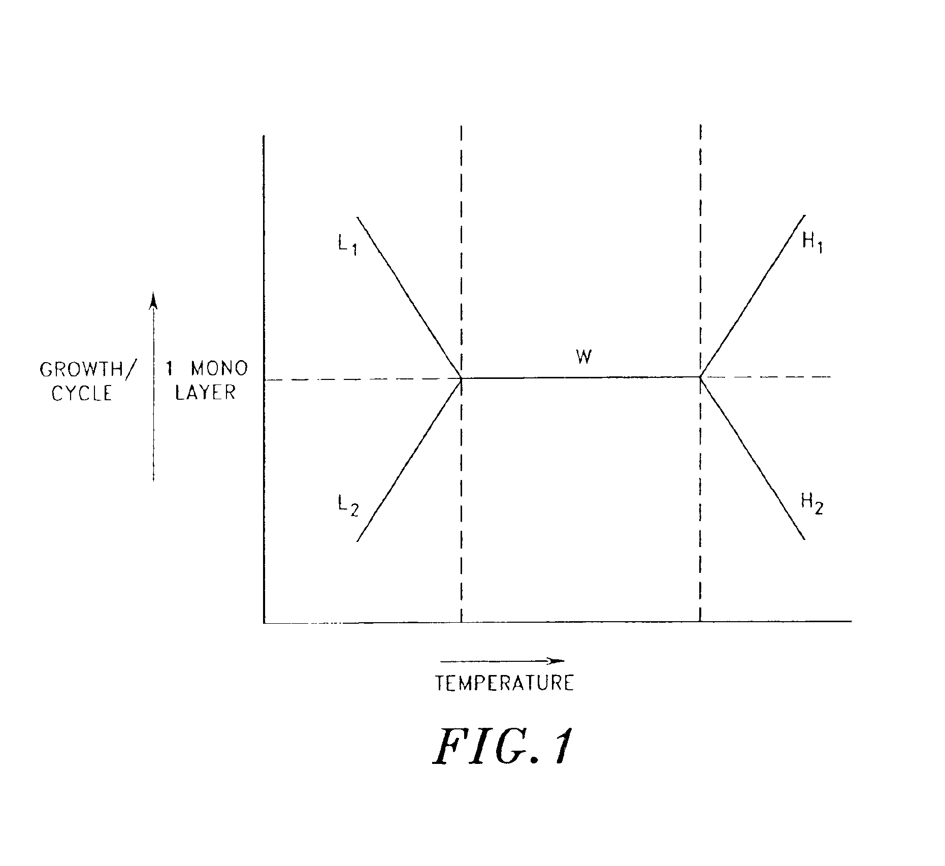
[0034]A growth curve corresponding to FIG. 2 has been obtained for the growth of ZnSe from alternating pulses of elemental Zn and Se. A growth of about 1 monolayer per cycle occurs in the temperature range of 250° C. to 350° C. (Suntola, T. 1994. “Atomic Layer Epitaxy,” in Handbook of Crystal Growth 3, Thin Films and Epitaxy, Part B: Growth Mechanisms and Dynamics, D. T. J. Hurle, Ed. Elsevier, Chapter 14, pp. 601-663). Thus, the temperature of the substrate is preferably set between 250° C. and 350° C. while the temperature of the reactor walls are preferably set above 350° C. (resulting in reduced growth on the walls). In general, the reactor walls are also set below the temperature at which the reactants thermally decompose. It is to be noted, however, that in this example the source chemicals are elements and in that respect they cannot thermally decompose, although Se8 molecules may fragment into smaller selenium molecules.

example 2

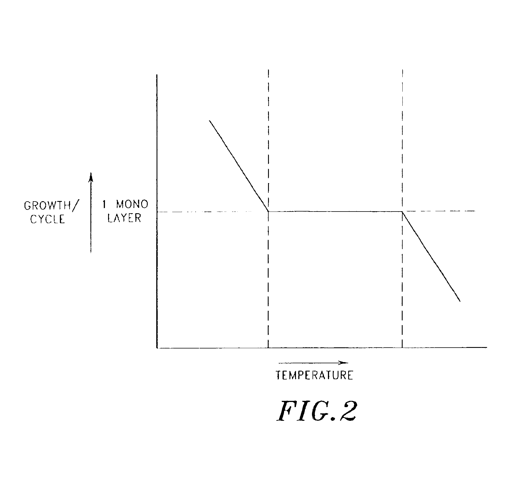
[0035]A growth curve according to FIG. 3 has been reported for the atomic layer deposition of GaAs from alternating pulses of trimethylgallium and arsine. A growth of about 1 monolayer occurs in the temperature range of 490° C. to 520° C. (Suntola, T. “Atomic Layer Epitaxy,” in Handbook of Crystal Growth 3, Thin Films and Epitaxy, Part B: Growth Mechanisms and Dynamics, D. T. J. Hurle, Ed. Elsevier, Chapter 14, pp. 601-663 (1994)).

[0036]In this situation, the substrate temperature is preferably set between 490° C. and 520° C. and the temperature of the reactor walls is preferably set below 490° C. (resulting in reduced growth on the walls). However, the temperature of the reactor walls is also preferably maintained above the temperature at which condensation of the reactants would occur.

example 3

[0037]A growth curve according to FIG. 4 has been reported for the ALD growth of SnO2 from alternating pulses of vaporized SnCl4 and H2O (Viirola and Niinistö, Thin Solid Films, 249:144-149 (1994)). The ALD growth rate was maximal at a substrate temperature of about 500° C. When the substrate temperature was decreased from 500° C. to 300° C., the growth rate of SnO2 dropped from 0.30 Å / cycle to about 0.12 Å / cycle.

[0038]In this case, where the ALD reaction is considered thermally driven, in the sense that ALD reactions are facilitated at higher temperatures and inhibited at lower temperatures, it is preferable to set the wall temperature at a lower level than the substrate temperature. The reaction chamber wall temperature is also preferably high enough to avoid the condensation of source chemicals on the walls, which can produce particles that are harmful for thin film processes. The maximum possible vapor pressure of the source chemical in a chamber depends on the coldest spot in t...


PUM

PropertyMeasurementUnit
Temperatureaaaaaaaaaa
Densityaaaaaaaaaa
Densityaaaaaaaaaa

Abstract

The present invention relates to improved methods and apparatus for atomic layer deposition (ALD) of thin films on substrates such as wafers and flat panel displays. The invention provides an ALD reactor comprising a first temperature regulating system to control the temperature of the substrate and a second temperature regulating system to independently control the temperature of the reaction chamber walls. The invention also provides a method for ALD of a film onto a substrate in a reaction chamber, in which the temperature of the substrate is maintained to maximize ALD on the substrate while the temperature of the reaction chamber walls is set to minimize film growth thereon, whether by ALD, condensation, physisorption or thermal decomposition. The temperature of the walls may be maintained at the same temperature as the substrate, or higher or lower than the substrate temperature, depending upon the particular reaction being used.

Description

[0001]This application is related to U.S. application Ser. Nos. 09 / 769,562 filed Jan. 25, 2001, now U.S. Pat. No. 6,579,374, and 09 / 568,077 filed May 10, 2000, now U.S. Pat. No. 6,562,140.FIELD OF THE INVENTION[0002]This invention relates to the field of reactor design for atomic layer deposition of thin films onto substrates such as wafers and flat panel displays.BACKGROUND OF THE INVENTION[0003]In atomic layer deposition (ALD), a substrate placed in a reaction space is subjected to alternating pulses of at least two different reactants suitable for producing a desired thin film on the substrate. When the substrate is exposed to a pulse of the first reactant, a monolayer of the first reactant is chemisorbed on the surface of the substrate until all of the available surface sites are occupied with an adsorbed portion of a reactant molecule and saturation occurs. The surface sites may be occupied by the whole of or by a fragment of a vapor-phase reactant molecule, such as when a meta...

Claims


Application Information

Patent Timeline
IPC IPC(8): C23C16/30C23C16/44C23C16/46C23C16/40C23C16/455B01J19/00H01L21/205
CPCC23C16/301C23C16/305C23C16/403C23C16/405C23C16/407C23C16/44C23C16/45525C23C16/45544C23C16/46
Inventor BONDESTAM, NIKLASLINDFORS, SVEN
Owner ASM INTERNATIONAL
Why Eureka
Try Eureka