Silicon-rich low thermal budget silicon nitride for integrated circuits

a silicon nitride, low thermal budget technology, applied in the direction of semiconductor/solid-state device details, semiconductor devices, electrical apparatus, etc., can solve the problems of boron penetration and boron-doped poly depletion, destroying transistor performance, and reducing the efficiency of silicon nitrid

Inactive Publication Date: 2005-09-06
BELL SEMICON LLC
View PDF8 Cites 6 Cited by
  • Summary
  • Abstract
  • Description
  • Claims
  • Application Information

AI Technical Summary

Problems solved by technology

As such, hydrogen that is bonded to nitrogen, as opposed to being bonded to silicon, is more susceptible to becoming dissociated from its bond and migrating throughout and from the SiN film.
Such boron diffusion may result in boron penetration and boron-doped poly depletion.
Because of the relative activation energies, it has been found that only the N—H bonded hydrogen contributes to the above-mentioned anomalies that negatively impact the device.
In MOSFET technology, when conventional silicon nitride spacers are formed adjacent the poly gate, the hydrogen, prevalently bonded with nitrogen of the silicon nitride film and forming a weak bond therewith, breaks free and enhances boron diffusion during subsequent high-temperature processing operations such as the source / drain anneals typically carried out at temperatures within the range of 1000-1100° C. Such boron penetration into the transistor gate oxide or the transistor channel, shifts the Vt (threshold voltage) of the transistor at the least, and may completely destroy transistor performance.
Another mechanism in which un-bonded hydrogen negatively impacts device performance is boron-doped poly depletion.
In this manner, the hydrogen remains bonded to the silicon nitride film and does not enhance the aforementioned mechanisms of boron penetration and boron-doped poly depletion that negatively impact semiconductor devices.

Method used


Image

  • Silicon-rich low thermal budget silicon nitride for integrated circuits
  • Silicon-rich low thermal budget silicon nitride for integrated circuits
  • Silicon-rich low thermal budget silicon nitride for integrated circuits

Examples


Embodiment Construction

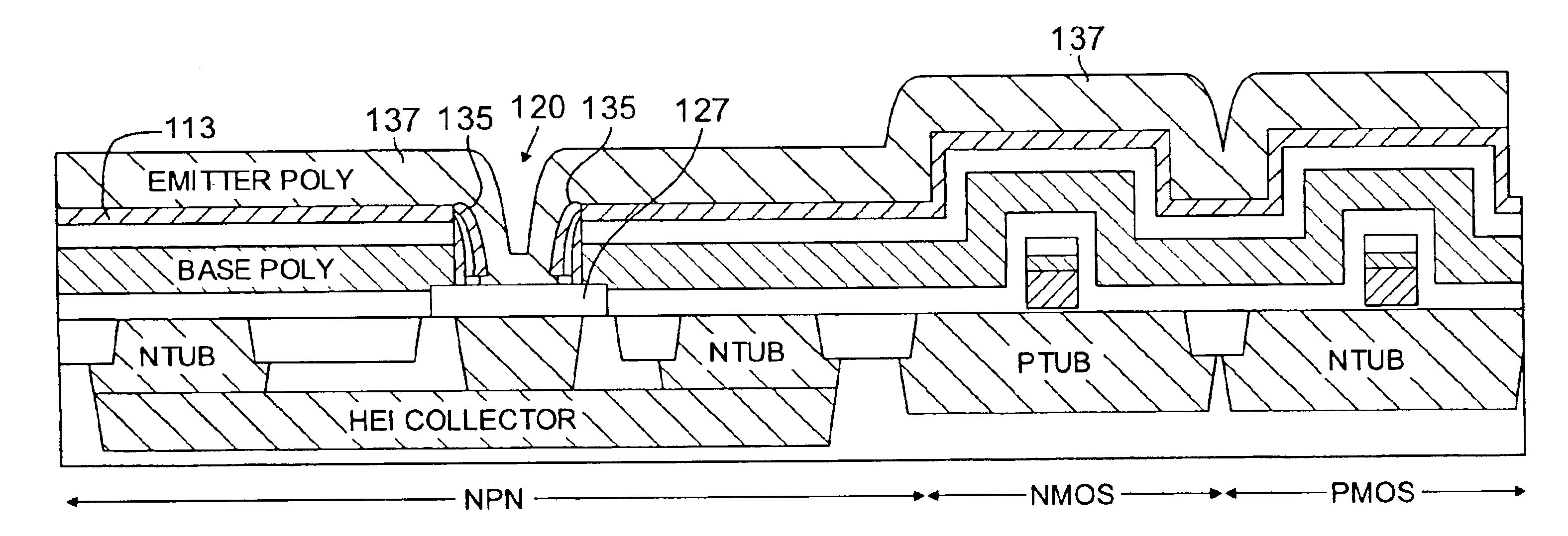
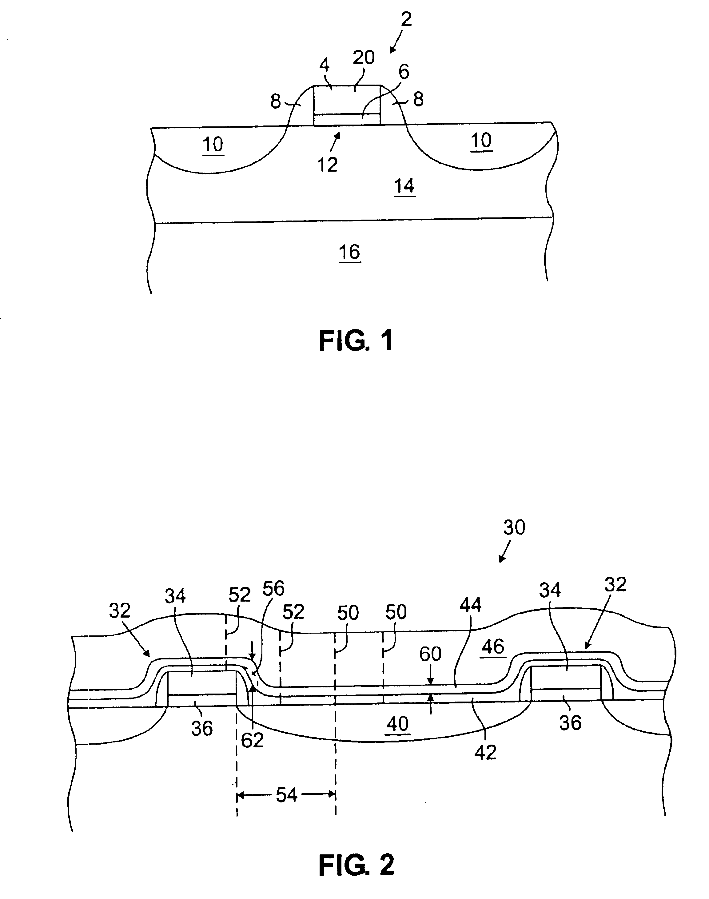
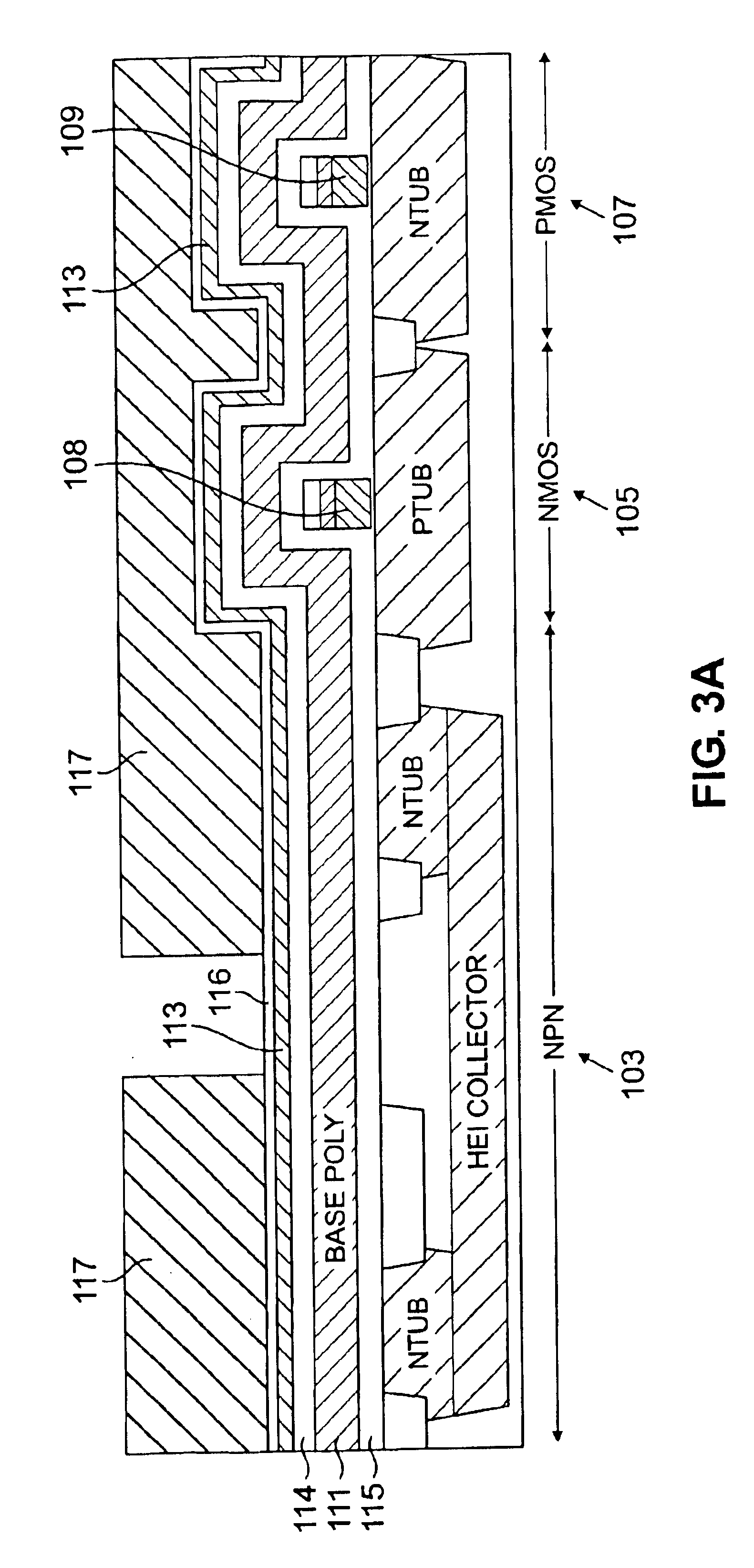
[0015]The present invention provides a silicon-rich SiN (silicon nitride) film. The present invention further provides various methods for forming the silicon-rich SiN film using various processes that advantageously include a relatively low thermal budget. Due in large part to the methods and source gases used to form SiN films, such SiN films, including the SiN films of the present invention, include hydrogen interstitiated within the film and complexing with the components of the film, namely, silicon and nitrogen. According to preferred embodiments of the invention, silicon-rich SiN films include an increased amount of hydrogen bonded in Si—H bonds and a decreased amount of hydrogen bound in N—H bonds, compared to conventional SiN films. In one embodiment the SiN film induces a higher portion of the hydrogen being bound to silicon than to nitrogen. Since Si—H bonds include a higher activation energy than N—H bonds, a lesser amount of hydrogen is able to become dissociated and di...


PUM

PropertyMeasurementUnit
temperaturesaaaaaaaaaa
temperatureaaaaaaaaaa

Abstract

A low-thermal budget, silicon-rich silicon nitride film may include a concentration of hydrogen in Si—H bonds being at least 1.5 times as great as a concentration of hydrogen in N—H bonds. The silicon nitride film suppresses boron diffusion in boron-doped devices when such devices are processed using high-temperature processing operations that conventionally urge boron diffusion. The low-thermal budget, silicon-rich silicon nitride film may be used to form spacers in CMOS devices, it may be used as part of a dielectric stack to prevent shorting in tightly packed SRAM arrays, and it may be used in BiCMOS processing to form a base nitride layer and/or nitride spacers isolating the base from the emitter. Furthermore the low-thermal budget, silicon-rich silicon nitride film may remain covering the CMOS structure while bipolar devices are being formed, as it suppresses the boron diffusion that results in boron penetration and boron-doped poly depletion.

Description

FIELD OF THE INVENTION[0001]The present invention relates most generally to semiconductor devices and methods for forming the same. More particularly, the present invention is related to a low thermal budget, silicon-rich SiN film used in various integrated circuit applications for suppressing boron penetration and boron depletion.BACKGROUND OF THE INVENTION[0002]Boron is a commonly favored P-type dopant in the semiconductor manufacturing industry and is commonly used in CMOS, BiPolar and BiCMOS technologies. Silicon nitride, films are used extensively in semiconductor manufacturing for various functions, various applications, and in various technologies. When SiN films are formed, using the various methods of formation, hydrogen is invariably incorporated into the film. For example, silane (SiH4) is a source gas commonly used as the silicon source in the various processes used to form silicon nitride films. The hydrogen incorporated within the SiN film forms bonds with both the sil...

Claims


Application Information

Patent Timeline
Patent Type & Authority Patents(United States)
IPC IPC(8): H01L21/02H01L21/70H01L21/336H01L21/8249H01L29/51H01L21/324H01L21/8238H01L29/40H01L21/331H01L21/28H01L21/318H01L21/8234H01L21/8244H01L27/06H01L27/088H01L27/11H01L29/732H01L29/737H01L29/78
CPCH01L21/324H01L21/823864H01L29/6659H01L29/518H01L29/6656H01L21/8249H01L21/28
Inventor CARROLL, MICHAEL SCOTTMA, YIPATEL, MINESH AMRATSANA, PEYMAN
Owner BELL SEMICON LLC
Why Eureka
Try Eureka