

Multi-layer dielectric and method of forming same
a technology of multi-layer dielectrics and dielectric layers, which is applied in the direction of electrical apparatus, semiconductor devices, semiconductor/solid-state device details, etc., can solve problems such as circuit failure, circuit failure, undesirable effects, etc., and achieve the effect of low deposition ra
- Summary
- Abstract
- Description
- Claims
- Application Information
AI Technical Summary
Benefits of technology
Problems solved by technology
Method used
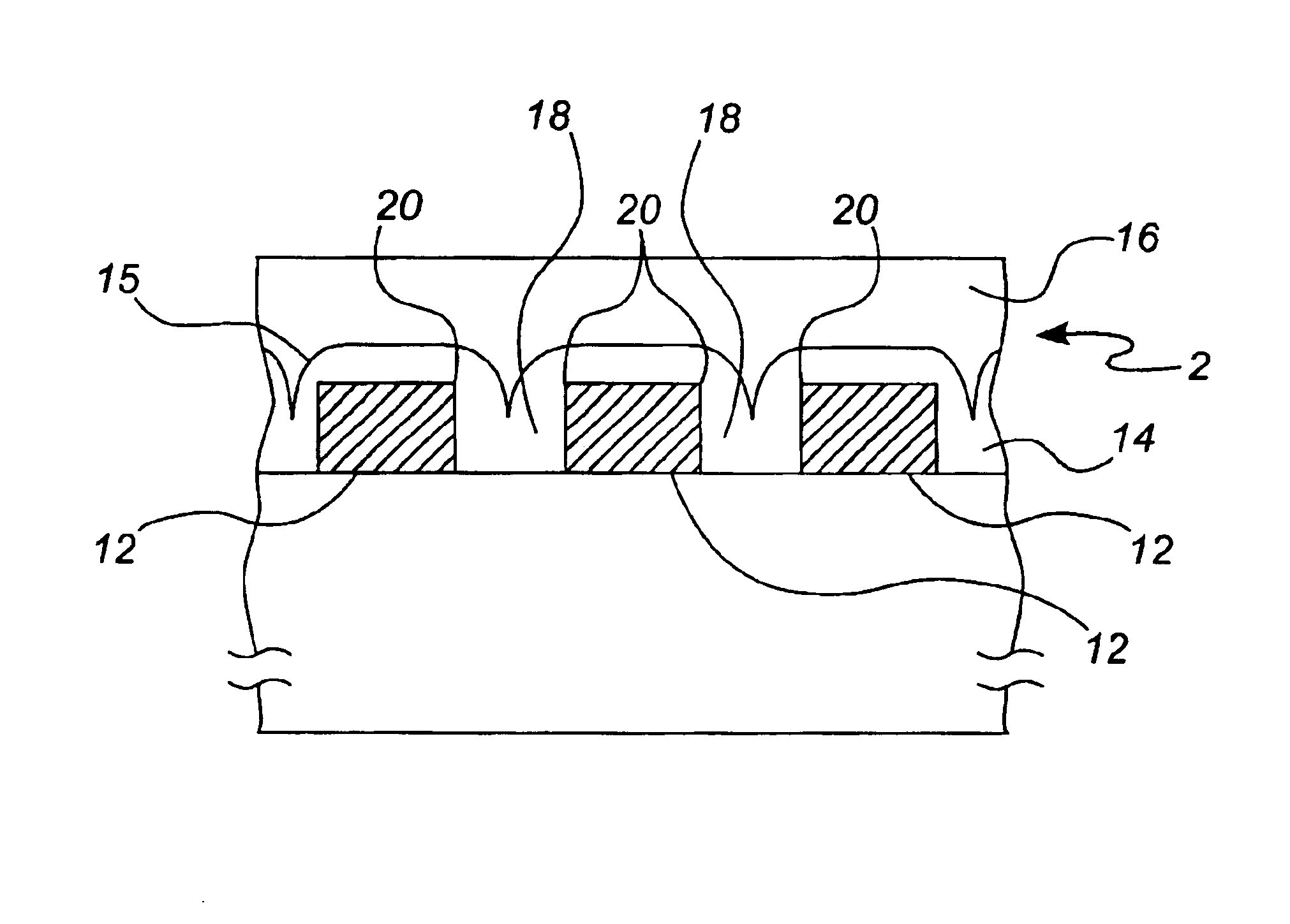
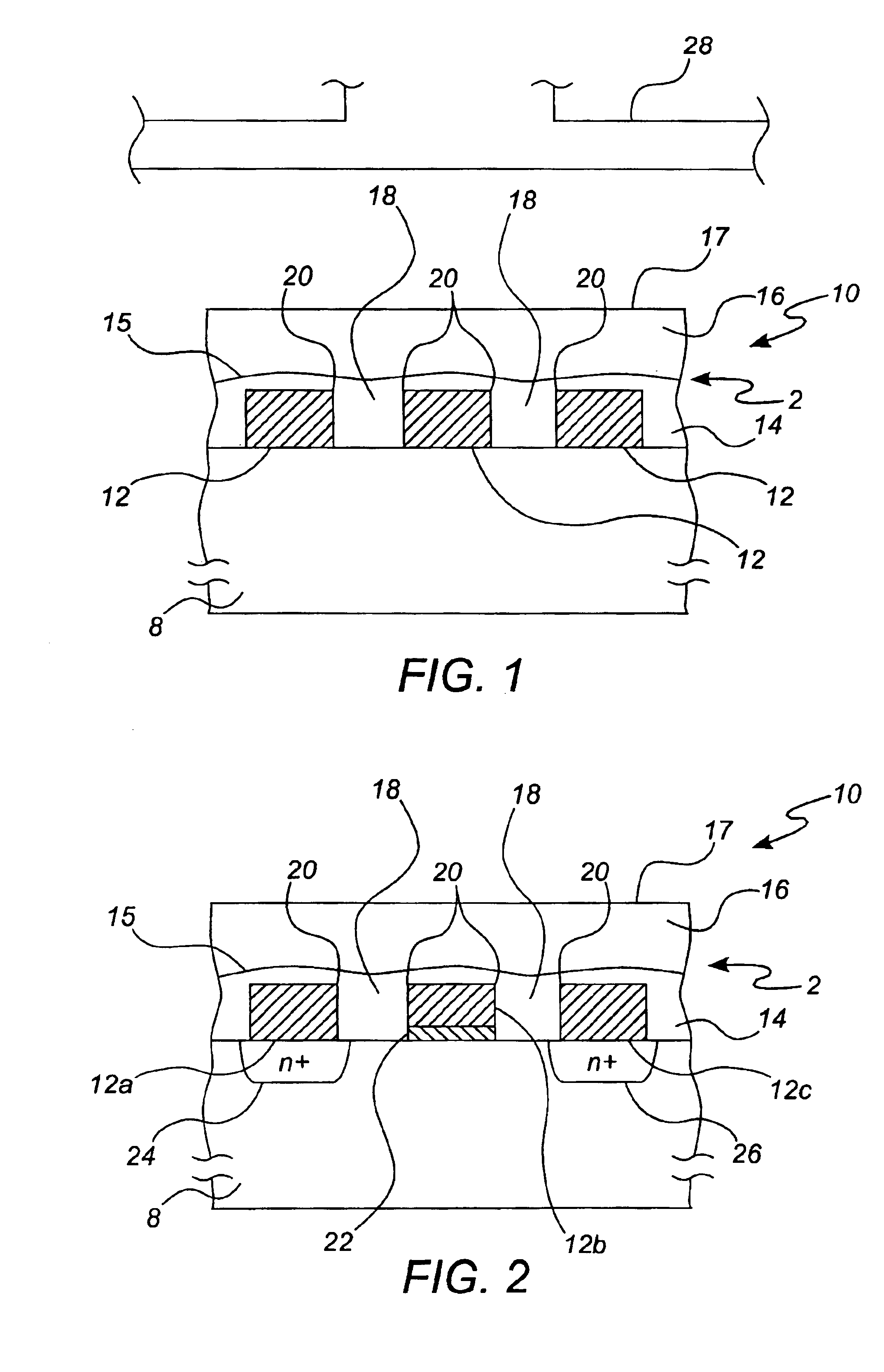
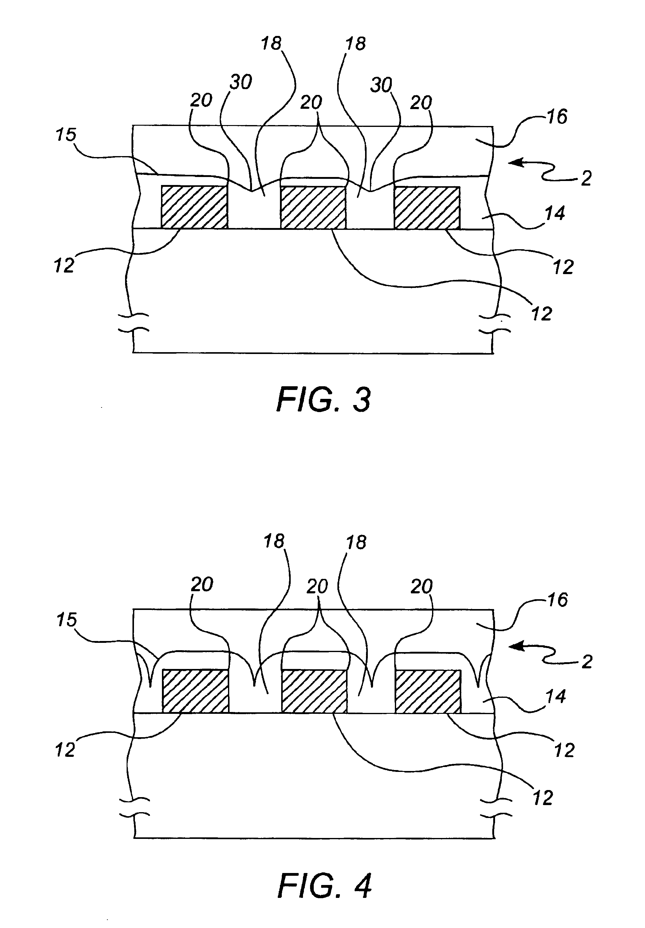
Image

Examples
examples
[0043]The below examples are provided to show the relationship between various process conditions and void sizes measured in scanning electron microscope (SEM) cross-sections for phosphosilicate glass (PSG) and borophosphosilicate glass (BPSG) films deposited under a variety of conditions. FIG. 5 shows the average void length versus deposition temperature for 6.9% PSG at 200 torr. FIG. 6 shows the average void length versus deposition pressure for 6.9 PSG at 530° C. FIG. 7 shows the average void area versus suseptor spacing for 2.7×7.2 BPSG. In each of FIGS. 5-7, all other deposition parameters were held constant. FIGS. 5-7 show that processes having lower deposition rates have better gap-fill characteristics (smaller voids) than processes with higher deposition rates.
[0044]FIG. 8 is a high level block diagram illustrating a system 50 including a first device 52, a bus 54, and a second device 56. The system 50 may be, for example, a memory system or a computer system. The first devi...
PUM
| Property | Measurement | Unit |
|---|---|---|
| aspect ratios | aaaaa | aaaaa |
| temperature | aaaaa | aaaaa |
| pressure | aaaaa | aaaaa |
Abstract
Description
Claims
Application Information