Solder pads for improving reliability of a package

Inactive Publication Date: 2005-09-06
UNITED MICROELECTRONICS CORP
View PDF15 Cites 26 Cited by
  • Summary
  • Abstract
  • Description
  • Claims
  • Application Information

AI Technical Summary

Benefits of technology

[0010]It is therefore a primary objective of the claimed invention to provide solder pads for improving reliability of a package.
[0011]According to the claimed invention, solder pads for improving reliability of a semiconductor package are provided. The package includes a substrate and/or a chip. The solder pad includes a plurality of first solder pads located on a surface of the substrate and/or the chip, and at least a second solder pad located on a predetermined region of the surface of the substrate and/or the chip. Each of the first solder pads has a first diameter. The second solder pad has a second diameter greater than the first diameter so as to sustain a stronger thermal stress on the subs

Problems solved by technology

However, a price of the ceramic substrate is high and a source of the ceramic substrate is limited, so that the plastic substrate with a low price and plentiful sources has become a mainstream material used in packages.
Nevertheless, a problem of non-uniform thermal stress always occurs in a package when using the plastic substrate.
As a resul

Method used


Image

  • Solder pads for improving reliability of a package
  • Solder pads for improving reliability of a package
  • Solder pads for improving reliability of a package

Examples


first embodiment

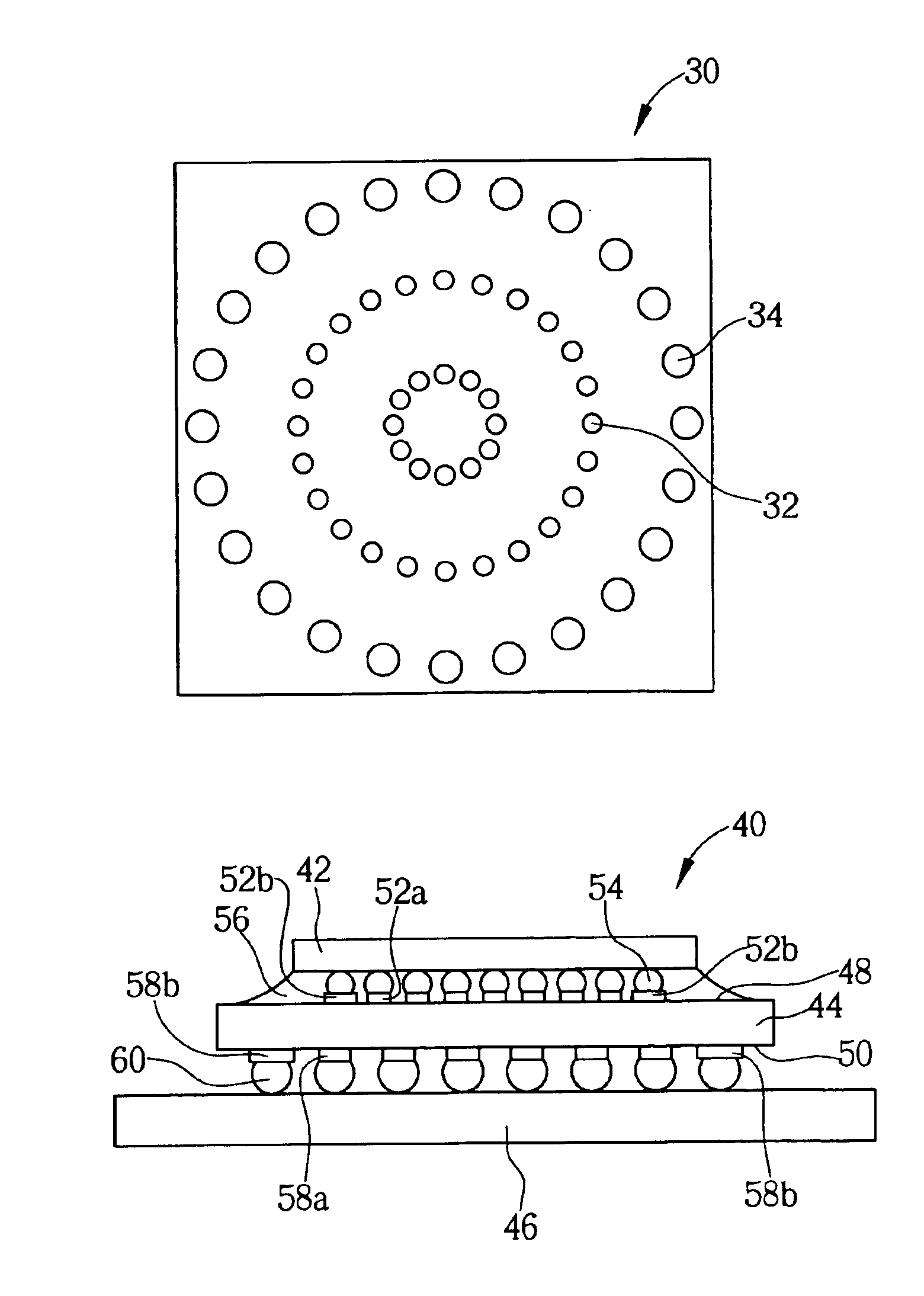
[0019]Please refer to FIG. 5 to FIG. 11. FIG. 5 to FIG. 11 are schematic diagrams for illustrating the solder pads of the embodiments according to the present invention. The solder pads with larger sizes are located on the high stress regions of a substrate and / or a chip in the present invention. The solder pads with larger sizes can sustain stronger thermal stress and mechanical strength. As shown in FIG. 5, FIG. 5 illustrates the solder pads of the A plurality of first solder pads 32 and a plurality of second solder pads 34 are located on a surface of a substrate and / or a chip 30. The first solder pads 32 are arranged in a matrix at a center region of the substrate 30. The second solder pads 34 are arranged at the four vertexes of the matrix formed by the first solder pads 32. The diameter of the second solder pad 34 is larger than that of the first solder pad 32. In order to ensure reliability of the package during the welding process, the height of the first solder pad 32 is eq...

second embodiment

[0020]Please refer to FIG. 6. FIG. 6 illustrates the solder pads of the present invention. As shown in FIG. 6, a plurality of first solder pads 32 and a plurality of second solder pads 34 are located on a surface of a substrate and / or a chip 30. The first solder pads 32 are arranged in a matrix at a center region of the substrate 30. The second solder pads 34 are located at the corners of the matrix formed by the first solder pads 32. In addition, the corners of the matrix include the four vertexes of the matrix and the positions around the vertexes of the matrix. The diameter of the second solder pad 34 is larger than that of the first solder pad 32. In order to ensure reliability of the package during the welding process, the height of the first solder pad 32 is equal or approximately equal to that of the second solder pad 34.

third embodiment

[0021]Please refer to FIG. 7. FIG. 7 illustrates the solder pads of the present invention. As shown in FIG. 7, a plurality of first solder pads 32 and a plurality of second solder pads 34 are located on a surface of a substrate and / or a chip 30. The first solder pads 32 are arranged in a matrix at a center region of the substrate and / or the chip 30. The second solder pads 34 are arranged at the regions near the four vertexes of the matrix formed by the first solder pads 32. For example, the second solder pads 34 are arranged at the positions around the four vertexes of the matrix, and no second solder pads 34 are located at the four vertexes of the matrix. The diameter of the second solder pad 34 is larger than that of the first solder pad 32. In order to ensure reliability of the package during the welding process, the height of the first solder pad 32 is equal or approximately equal to that of the second solder pad 34.


PUM

PropertyMeasurementUnit
Diameteraaaaaaaaaa
Circumferenceaaaaaaaaaa
Fatigue strengthaaaaaaaaaa

Abstract

Solder pads for improving reliability of a semiconductor package are provided. The package includes a substrate and/or a chip. The solder pad includes a plurality of first solder pads located on a surface of the substrate and/or the chip, and at least a second solder pad located on a predetermined region of the surface of the substrate and/or the chip. Each of the first solder pads has a first diameter. The second solder pad has a second diameter greater than the first diameter so as to sustain a stronger thermal stress on the substrate and/or the chip.

Description

BACKGROUND OF INVENTION[0001]1. Field of the Invention[0002]The present invention relates to solder pads of a package, and more particularly, to solder pads for improving reliability of a package.[0003]2. Description of the Prior Art[0004]High performance microelectronic devices often use solder balls or solder bumps for electrically and mechanically interconnection to other microelectronic devices. For instance, a very large scale integration (VLSI) chip may be connected to a circuit board or other next level packaging substrate by using solder balls or solder bumps. This connection technology is also referred to as “flip chip” technology. The flip chip technology is an area array connection technology and includes reflowing a body of solder onto a bond pad to form a solder bump, so as to electrically connect an IC die to a packaging board. The flip chip can break through limitations of traditional wire bonding, and the electrical performance is effectively improved due to a shorte...

Claims


Application Information

Patent Timeline
IPC IPC(8): H01L23/498H05K3/34
CPCH01L23/49816H01L23/49838H01L24/05H01L24/06H01L2224/05568H01L2224/05573H01L2224/06131H01L2224/06135H01L2224/0614H01L2224/06179H01L2224/16H01L2224/16225H01L2224/32225H01L2224/73204H01L2224/81192H01L2924/3511H05K3/3436H05K2201/094H05K2201/09418H05K2203/0465Y02P70/50H01L2924/00
Inventor CHEN, KUO-MING
Owner UNITED MICROELECTRONICS CORP
Why Eureka
Try Eureka