Noise reduction circuit for CCD output signal

a noise reduction circuit and output signal technology, applied in the field of noise reduction circuits, can solve the problems of hardly getting enough noise reduction effect in the noise reduction circuit, reducing sensitivity, and reducing the dynamic range, so as to reduce the noise in the output signal of ccd, reduce the dynamic range, and reduce the summing circuit

Active Publication Date: 2005-09-06
PANASONIC CORP
View PDF2 Cites 26 Cited by
  • Summary
  • Abstract
  • Description
  • Claims
  • Application Information

AI Technical Summary

Benefits of technology

[0035]The configuration described above has following effects. A noise in a signal-level period is canceled by that in a feedthrough-level period. The noise in an output signal of CCD is thus reduced. The lower level signal between the output signal of CCD and the pulse signal, and the lower level signal between the delay signal, into which the output signal gets delayed, and the pulse signal are selected respectively, and these selected signals are summed. Even if CCD has a large number of pixels a short pixel period, the summing circuit and the mixing circuits may have a narrow dynamic range. The power consumption of each of the pulse generator, the summing circuit, and the mixing circuits is reduced. Since the pulse generator outputs only one type of pulse signal, the circuit may be simple, and the power consumption of the circuit is more reduced. In particular, since the pulse generator generates the pulse signal of a small peak-to-peak value, even if CCD has a large number of pixels and a short pixel period, the power consumption of the pulse generator is greatly reduced.

Problems solved by technology

In fact, when the resolution of a camera is getting higher, problems like a decrease in sensitivity and a decrease in a dynamic range are coming up because an amount of a signal charge of CCD decreases.
Therefore, the noise reduction circuit hardly gets enough noise reduction effect.
Because an increase in the number of pixels of CCD makes any noise reduction circuit described above needs broadband circuits, the power consumption of the circuit is increased.
Furthermore, since pulse generator 65 shown in FIG. 10 has to generate pulse signal Yd with a large peak-to-peak value, the power consumption of the generator is increased.

Method used


Image

  • Noise reduction circuit for CCD output signal
  • Noise reduction circuit for CCD output signal
  • Noise reduction circuit for CCD output signal

Examples


embodiment 1

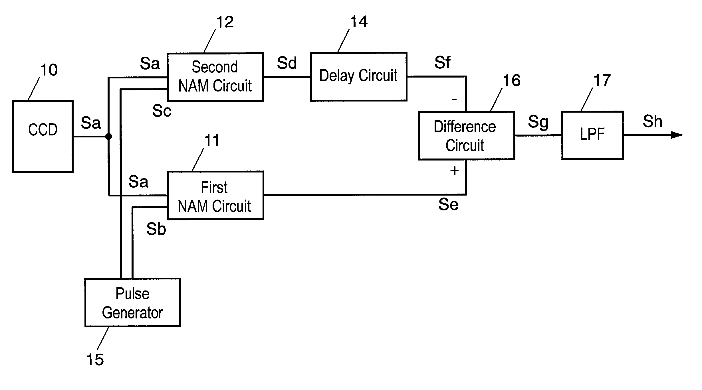
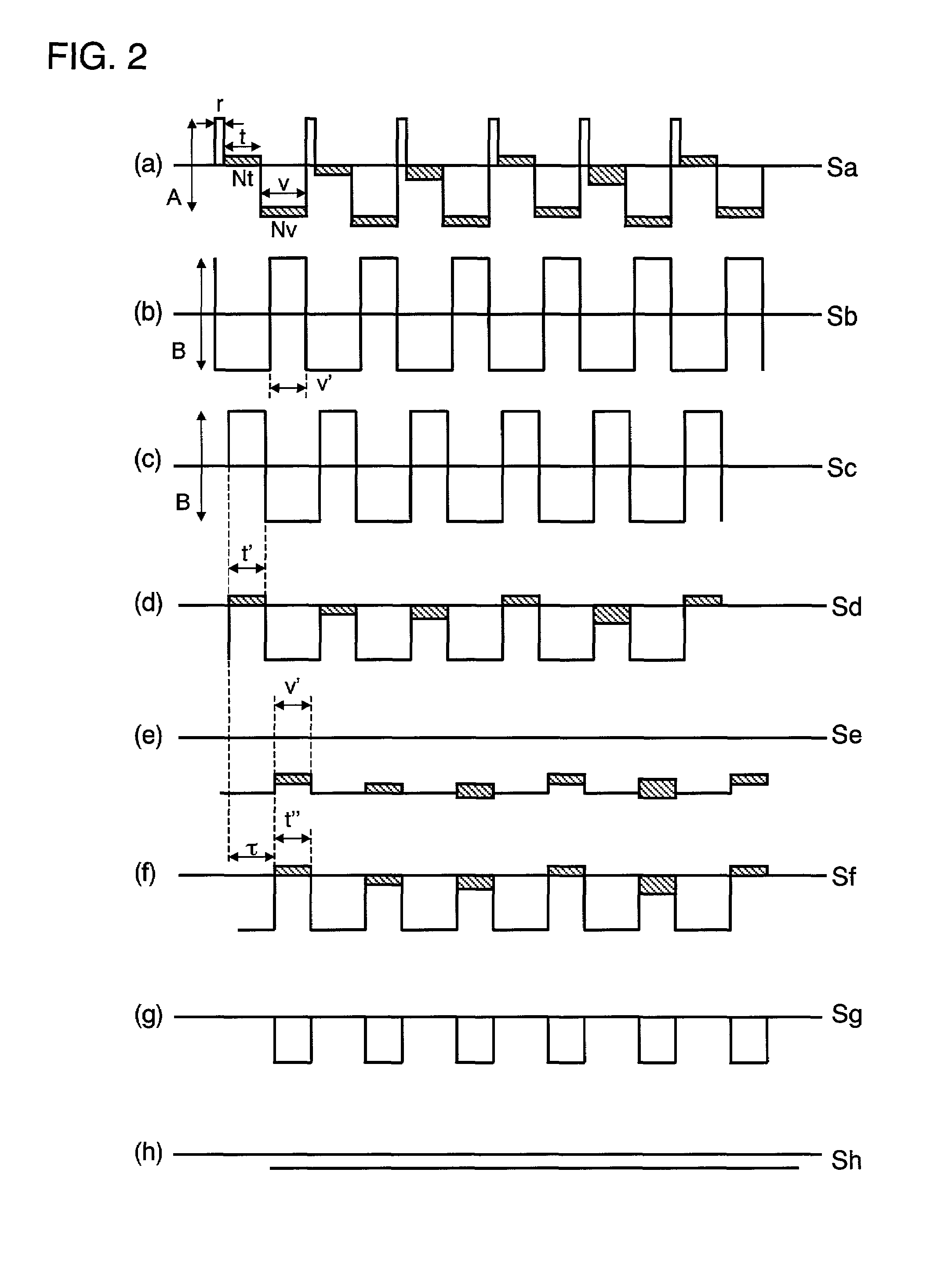
[0047]A noise reduction circuit in accordance with embodiment 1 of the present invention is described hereinafter with reference to FIG. 1, FIG. 2, and FIG. 7.

[0048]FIG. 1 is a block diagram illustrating a noise reduction circuit in accordance with embodiment 1. An output terminal of charge coupled device (CCD) 10 is connected to one input terminal of first non-additive mixing (NAM) circuit 11 and one input terminal of second NAM circuit 12. Output terminals of pulse generator 15 are connected to another input terminal of first NAM circuit 11 and another input terminal of second NAM circuit 12 respectively. Pulse generator 15 outputs two types of pulse signals Sb and Sc which have the same period that output signal Sa of CCD 10 has. A difference between the two types of pulse signals Sb and Sc is described later with reference to FIG. 2.

[0049]First pulse signal Sb of these two type signals Sb and Sc is input to first NAM circuit, and second pulse signal Sc is input to second NAM cir...

embodiment 2

[0069]A noise reduction circuit in accordance with embodiment 2 of the present invention is described hereinafter with reference to FIG. 3, FIG. 4, and FIG. 7.

[0070]First, FIG. 3 is a block diagram illustrating a noise reduction circuit in accordance with embodiment 2. An output terminal of CCD 20 is connected to one input terminal of first NAM circuit 21 and an input terminal of delay circuit 24. An output terminal of delay circuit 24 is connected to one input terminal of second NAM circuit 22. Delay circuit 24 receives CCD output signal Ta of CCD 20, delays signal Ta, and outputs output delay signal Tb to second NAM circuit 22. An output terminal of pulse generator 25 is connected to another input terminal of first NAM circuit 21 and another input terminal of second NAM circuit 22. Pulse generator 25 outputs one type of pulse signal Tc which has the same period that an output signal Ta of CCD 20 has.

[0071]First NAM circuit 21 selects and outputs a lower level signal between CCD ou...

embodiment 3

[0090]A noise reduction circuit in accordance with embodiment 3 of the present invention is described hereinafter with reference to FIG. 5, FIG. 6, and FIG. 7.

[0091]FIG. 5 is a block diagram illustrating a noise reduction circuit in accordance with embodiment 3. An output terminal of CCD 30 is connected to one input terminal of first NAM circuit 31 and an input terminal of inverting circuit 33. An output terminal of inverting circuit 33 is connected to an input terminal of delay circuit 34, and an output terminal of delay circuit 34 is connected to one input terminal of second NAM circuit 32. Inverting circuit 33 inverts output signal Ua of CCD 30, and outputs inverted signal Ub. Delay circuit 34 receives inverted signal Ub from inverting circuit 33, delays signal Ub, and outputs signal Uc to second NAM circuit 32. An output terminal of pulse generator 35 is connected to another input terminal of first NAM circuit 31 and another input terminal of second NAM circuit 32. Pulse generat...


PUM


Abstract

A noise reduction circuit with high noise reduction effect and low power consumption for a high resolution charge coupled device (CCD) as well as for a usual resolution CCD is provided. A delay circuit delays an CCD output signal, and a pulse generator outputs a pulse signal having the same period that the CCD output signal has. A part of period during which the pulse signal is at a high level overlaps with a signal-level period oh the CCD output signal. A first non-additive mixing (NAM) circuit selects and output a lower level signal between the CCD output signal and the pulse signal. A second NAM circuit selects and outputs a lower level signal between the output signal from the delay circuit and the pulse signal. A difference circuit calculates difference between an output signal of the first NAM circuit and an output signal of the second NAM circuit. A delay time of the delay circuit is set so that a feedthrough-level period of an output signal of the delay circuit overlaps with a signal-level period of the CCD output signal.

Description

FIELD OF THE INVENTION[0001]The present invention relates to a noise reduction circuit, and more particularly, a noise reduction circuit to reduce noise in an output of a charge coupled device (CCD).BACKGROUND OF THE INVENTION[0002]A charge coupled device (CCD) is usually used as an image-picking device, and has an advantage over an image pickup tube. The advantage is compact, lightweight, low power consumption, and highly reliable. CCD has further advantages of no distortion and no sticking. Therefore, CCD is used for consumer camcorders at a first stage. In recent years, CCD is in general used for various kinds of cameras up to broadcast cameras to which a high visual quality is required.[0003]In fact, when the resolution of a camera is getting higher, problems like a decrease in sensitivity and a decrease in a dynamic range are coming up because an amount of a signal charge of CCD decreases. For solving such problems and getting high quality images with high resolution, noise red...

Claims


Application Information

Patent Timeline
Patent Type & Authority Patents(United States)
IPC IPC(8): H04N5/335H04N5/217H04N5/341H04N5/365H04N5/372H04N5/376H04N5/378
CPCH04N5/359H04N5/372H04N25/62H04N25/71
Inventor MINE, TADAMI
Owner PANASONIC CORP
Why Eureka
Try Eureka