Systems, methods, and apparatuses for optically pumped vertical cavity surface emitting laser devices

a laser device and vertical cavity technology, applied in the direction of lasers, semiconductor laser structural details, semiconductor lasers, etc., can solve the problem that the commercial success of electrical pumping to achieve photon emission at long wavelengths is not good enough

Inactive Publication Date: 2005-09-06
JDS UNIPHASE CORP
View PDF51 Cites 54 Cited by
  • Summary
  • Abstract
  • Description
  • Claims
  • Application Information

AI Technical Summary

Benefits of technology

[0023]FIG. 11B is a magnified cross-sectional view and ray diagram illustration of automatic power control of a surface emitting semiconductor laser in response to power monitoring by a photodiode.

Problems solved by technology

However, achieving photon emission at long wavelengths using electrical pumping has not been commercially successful due to a number of disadvantages.

Method used


Image

  • Systems, methods, and apparatuses for optically pumped vertical cavity surface emitting laser devices
  • Systems, methods, and apparatuses for optically pumped vertical cavity surface emitting laser devices
  • Systems, methods, and apparatuses for optically pumped vertical cavity surface emitting laser devices

Examples


first embodiment

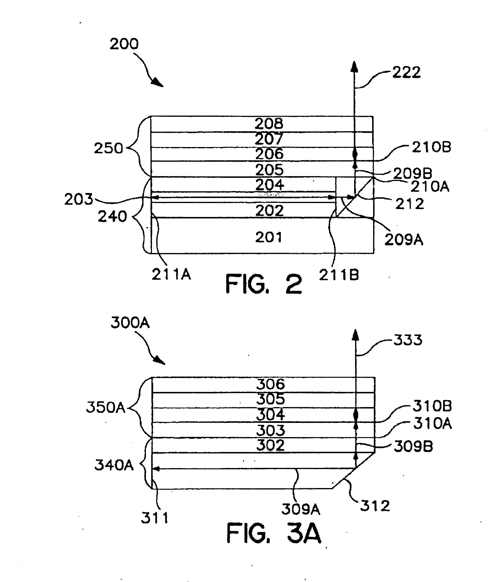
[0052]Referring now to FIG. 2, an integrated optically pumped VCSEL 200 as the invention is illustrated. The integrated optically pumped VCSEL 200 includes a short wavelength in-plane semiconductor laser, the edge-emitting laser 240, integrated with a long wavelength VCSEL 250. The edge emitting (EE) laser 240 can emit a laser beam (i.e. photons) at a wavelength over a range from 600 nm to 1110 nm. The edge emitting laser 240 will typically emit photons having wavelengths of 780 nm, 850 nm, or 980 nm. The laser beam 209A is steered by a beam steering element 212 towards the long wavelength VCSEL 250 to optically pump it. In response to the optical pumping, the long wavelength VCSEL 250 emits a laser beam at a wavelength over a range from 1250 nm to 1650 nm. The long wavelength VCSEL 250 typically emits a laser bean having a wavelength of 1300 nm or 1550 nm. The beam steering element 212 can be a mirror, an optical grating or other reflecting surface. The beam steering element 212 in...

fifth embodiment

[0070]Referring now to FIG. 3D, a fifth embodiment, integrated optically pumped VCSEL 300D is illustrated. The integrated optically pumped VCSEL 300D includes the in-plane surface emitting laser 340B and the long wavelength VCSEL 350D. Integrated optically pumped VCSEL 300D has the same in-plane surface emitting laser 340B as does VCSEL 300B with the beam steering elements 312A and 312B. Instead of portion 313 or 314, the long wavelength VCSEL 350D has portion 315 removed from the material of the distributed Bragg reflector (DBR) 305 and the substrate 306. This causes a single laser beam 333 to be emitted from the surface of the long wavelength VCSEL 350D. Otherwise, similarly numbered elements of the in-plane surface emitting laser 340B and the VCSEL 350D are similar to those previously described with respect to FIG. 3B and the integrated optically pumped VCSEL 300B.

[0071]Referring now to FIG. 3E, the integrated optically pumped VCSEL 300E is illustrated. The integrated optically p...

seventh embodiment

[0072]Referring now to FIG. 3F, the integrated optically pumped VCSEL 300F is illustrated. The integrated optically pumped VCSEL 300F includes the in-plane surface emitting laser 340C and the long wavelength VCSEL 350F. The in-plane surface emitting laser340C includes its own substrate 301 and the beam steering elements 312A and 312B. The long wavelength VCSEL 350F has its substrate 306 removed and instead of portions 313, 314, 315, or 316, a portion 317 is removed from the distributed Bragg reflector DBR 303, active area 304, and DBR 305. FIG. 3F illustrates how either one of the substrate for the in-plane surface emitting laser 340 or the substrate for the long wavelength VCSEL 350 can be removed.

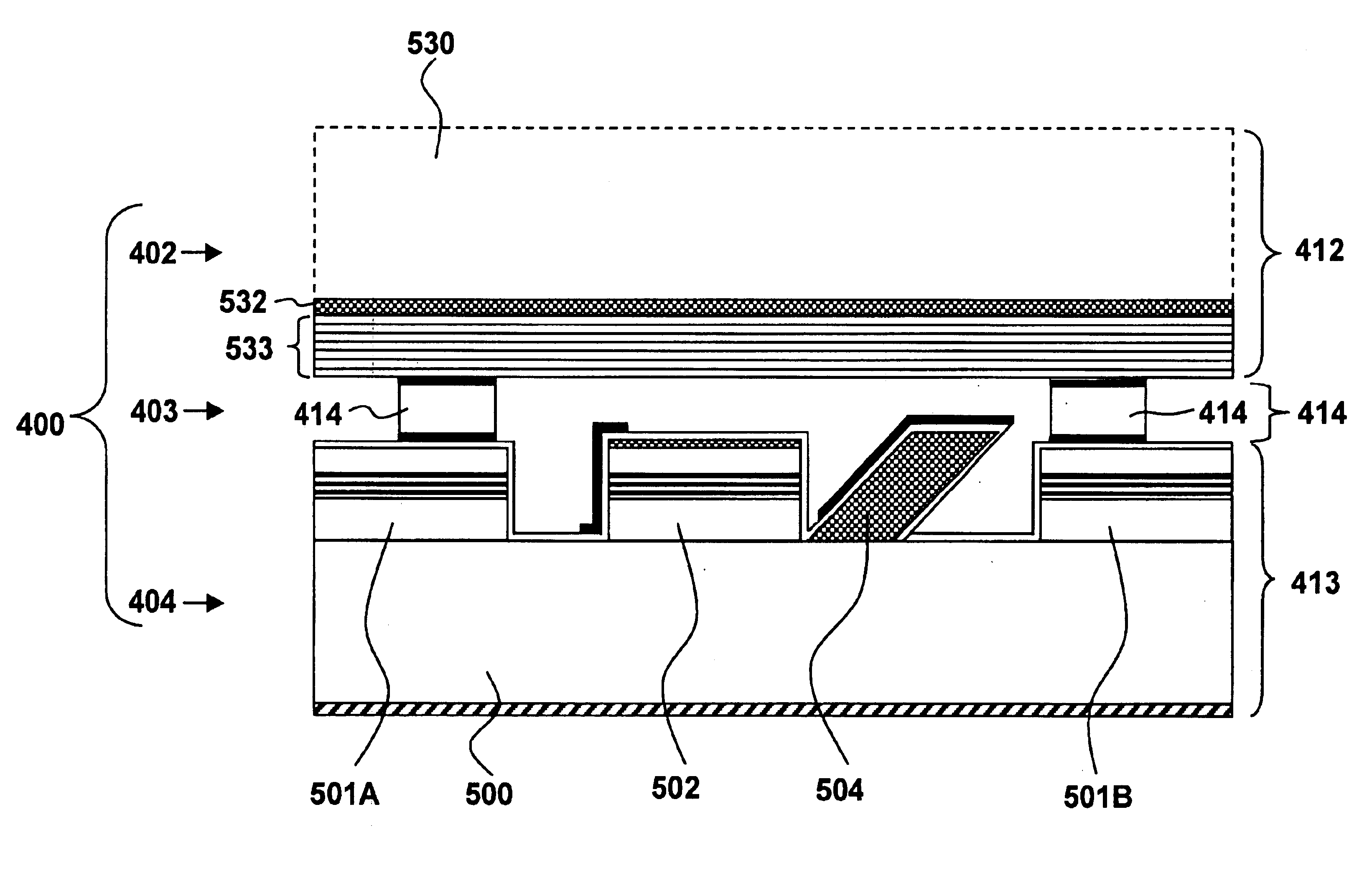
[0073]An edge emitting pump laser may be monolithically formed out of a semiconductor wafer and coupled to a long-wavelength VCSEL formed out of another semiconductor wafer to generate a monolithic integrated optically pumped long wavelength VCSEL.

[0074]Referring now to FIG. 4A, an explod...


PUM


Abstract

Monolithic integrated vertical-cavity surface-emitting laser devices are disclosed including an edge-emitting semiconductor pump laser (PL), an optically-pumped vertical-cavity surface-emitting laser (VCSEL), and a means for deflecting and shaping the output beam of the pump laser to optically excite the VCSEL. The optically-pumped VCSEL structure may be adapted to include a resonant cavity with multiple fixed wavelengths, or a resonance cavity whose wavelength is continuously tunable. Wafer level manufacturing techniques are also disclosed.

Description

CROSS REFERENCE TO RELATED APPLICATIONS[0001]This application is a continuation-in-part application and claims the benefit of U.S. application Ser. No. 10 / 175,338, filed Jun. 18, 2002 by inventors Wenbin Jiang et al, now U.S. Pat. No. 6,580,741, which is a divisional of U.S. application Ser. No. 09 / 430,570, filed Oct. 29, 1999 by inventors Wenbin Jiang et al, now issued as U.S. Pat. No. 6,424,669, all of which are to be assigned to E20 Communications, Inc.FIELD OF THE INVENTION[0002]The invention relates generally to semiconductor lasers. More particularly, the invention relates to vertical cavity surface emitting lasers.BACKGROUND OF THE INVENTION[0003]Semiconductor lasers have become more important. One of the most important applications of semiconductor lasers is in communication systems where fiber optic communication media is employed. With growth in electronic communication, communication speed has become more important in order to increase data bandwidth in electronic communi...

Claims


Application Information

Patent Timeline
Patent Type & Authority Patents(United States)
IPC IPC(8): H01S5/00H01S5/026H01S5/04H01S5/06H01S5/18H01S5/02H01S5/062H01S5/183
CPCH01S5/026H01S5/041H01S5/0215H01S5/0216H01S5/0265H01S5/0608H01S5/06216H01S5/06226H01S5/1085H01S5/18H01S5/18311
Inventor CHENG, JULIANSHIEH, CHAN-LONGMURTY, M. V. RAMANALEE, HSING-CHUNG
Owner JDS UNIPHASE CORP
Why Eureka
Try Eureka