UV nanoimprint lithography process using elementwise embossed stamp and selectively additive pressurization

a technology of nanoimprinting and lithography, applied in photomechanical treatment, instruments, electrical equipment, etc., can solve the problems of difficult multi-layer alignment, liable to damage to previously produced nanostructures, and difficult multi-layer alignment, so as to achieve fast form high-precision and high-quality nanostructures, and high-quality nanostructures

Inactive Publication Date: 2005-09-13
KOREA INST OF MASCH & MATERIALS
View PDF5 Cites 92 Cited by
  • Summary
  • Abstract
  • Description
  • Claims
  • Application Information

AI Technical Summary

Benefits of technology

[0015]It is an advantage of the present invention to provide a UV nanoimprint lithography process that uses an elementwise embossed stamp, which has formed on one side thereof element stamps divided by grooves, in a UV nanoimprint lithography process such that residual resist flows into the grooves between the element stamps during the lithography process. As a result, each element stamp is completely filled, and high-precision and high-quality nanostructures can be quickly formed on a large substrate.
[0016]It is another advantage of the present invention to provide a UV nanoimprint lithography process in which supplementary pressure is selectively applied in the lithography process in the case where resist is insufficiently or non-uniformly imprinted as a result of flatness errors of a stamp and a substrate, thereby enabling the use of large stamps to quickly form high-precision and high-quality nanostructures on a large substrate.
[0017]The UV nanoimprint lithography process for forming nanostructures on a substrate includes depositing a resist on a substrate; contacting a stamp having formed-thereon stamp nanostructures at areas corresponding to where nanostructures on the substrate are to be formed to an upper surface of the resist, and applying a predetermined pressure to

Problems solved by technology

In the development of semiconductor devices requiring multi-layer operations, thermal deformation caused by the high temperatures makes it difficult to successfully perform the multi-layer alignment.
Further, in order to perform imprinting of a resist with a high viscosity, a high pressure approximately as high as 30 bar is needed, which is liable to damage to the previously produced nanostructure.
An opaque stamp used in these processes makes the multilayer alignment even harder.
Although nanostructures of the stamp are quickly filled due to the small area of the stamp, the need to repeatedly align the stamp and perform multiple imprinting processes for a substrate increases th

Method used


Image

  • UV nanoimprint lithography process using elementwise embossed stamp and selectively additive pressurization
  • UV nanoimprint lithography process using elementwise embossed stamp and selectively additive pressurization
  • UV nanoimprint lithography process using elementwise embossed stamp and selectively additive pressurization

Examples


first embodiment

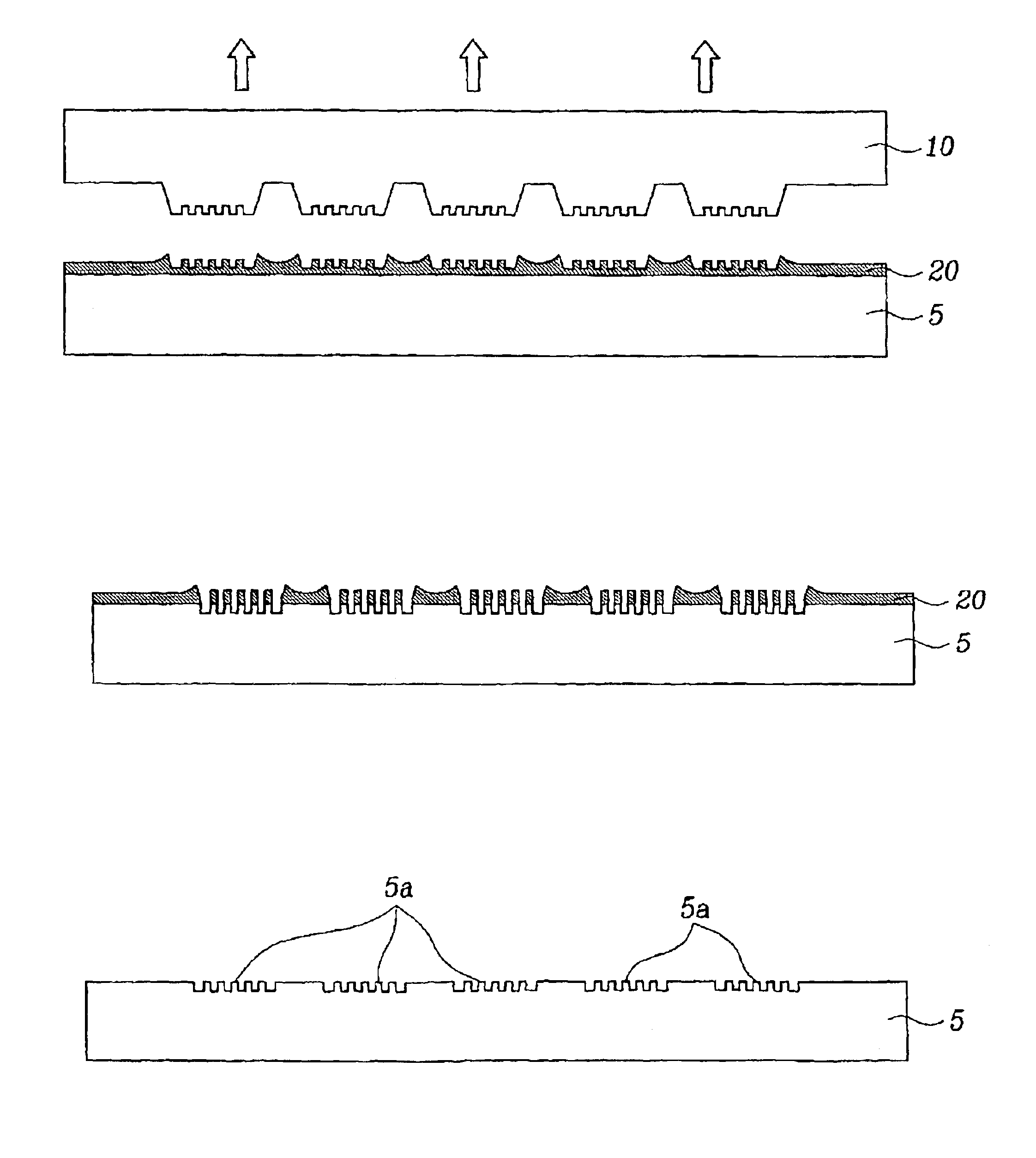
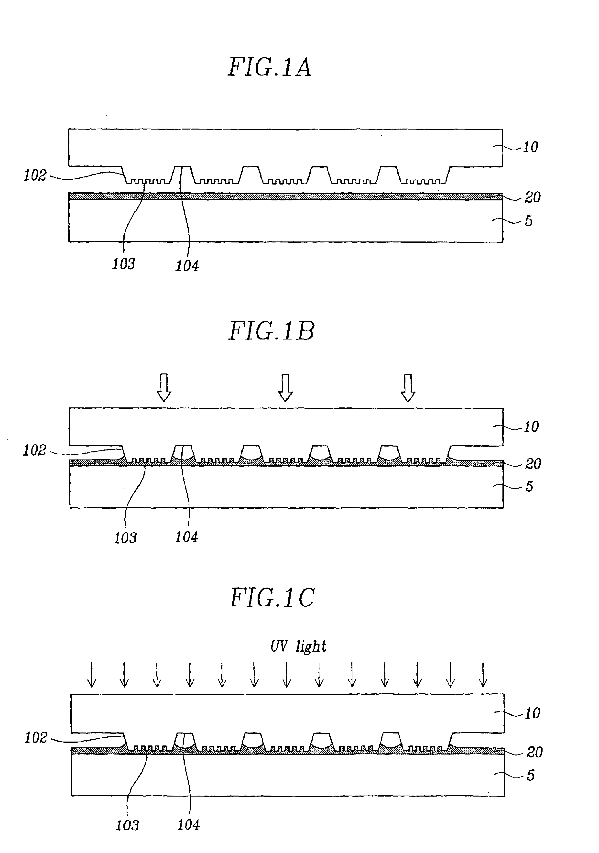
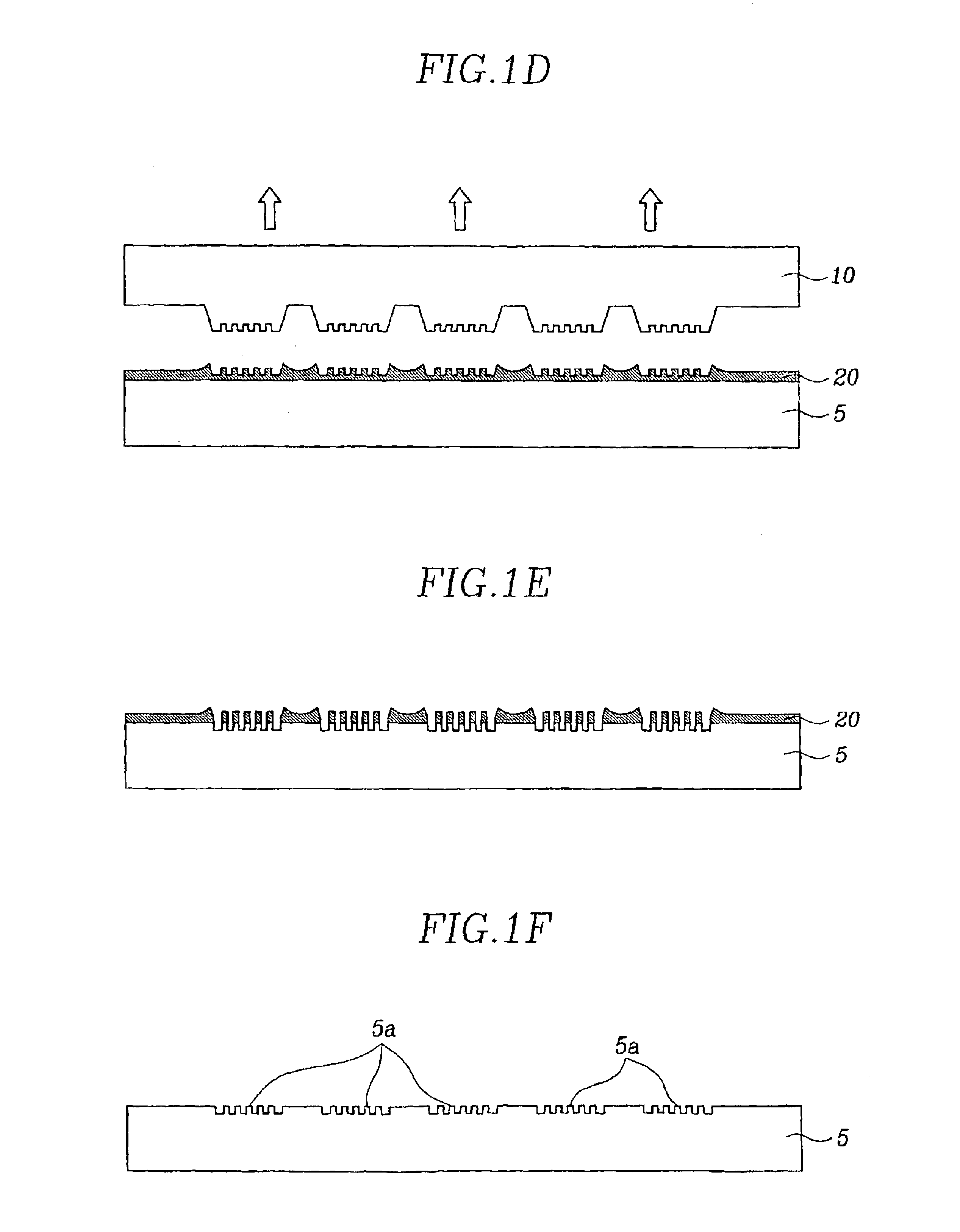
[0065]FIG. 2 is a top view of the elementwise embossed stamp 10 according to the present invention, and FIG. 3 is a sectional view taken along line A—A of FIG. 2.

[0066]As shown in FIGS. 2 and 3, the element stamps 102 arranged on the stamp 10 are embossed thereon, and the grooves 104 are formed between adjacent element stamps 102. Further, the nanostructures 103 are formed on each element stamp 102. The nanostructures 103 are formed using a microfabrication process; such as electron-beam lithography.

[0067]It is preferable that a depth hG of the grooves 104 is 2 to 1000 times a depth hS of the nanostructures 103. If the depth hG of the grooves 104 is less than 2 times the depth hS of the nanostructures 103, the minimal difference with the depth hS of the nanostructures 103 is such that the resist flowing into the grooves 104 reaches bottom surfaces thereof such that the function of the grooves 104 (i.e., receiving all residual resist) is unable to be realized. On the other hand, if t...

second embodiment

[0074]FIGS. 5A to 5D are sectional views used to describe processes for embossing element stamps by etching an elementwise embossed stamp according to the present invention.

[0075]To manufacture an elementwise embossed stamp 30 of the second embodiment of the present invention, a UV-transparent material such as quartz, glass, sapphire, or diamond is formed into a plate 6. Using the microfabrication process such the electron beam lithography on one side of the plate 6, nanostructures 303 are carved into the plate 6 at predetermined intervals, that is, at areas corresponding to where element stamps 302 are to be formed.

[0076]Next, a UV-curable resin layer 34 is deposited on the stamp 6 covering the nanostructures 303. A mask 36 having a pattern that blocks areas where the element stamps 302 are to be formed and exposes all other areas is placed at a predetermined distance from the surface of the plate 6 on which the nanostructures 303 are formed. UV rays are then irradiated onto the pl...

sixth embodiment

[0096]FIG. 20 is a top view used to show incompletely compressed resist areas when resist droplets are dispensed on a substrate using a multi-dispensing method, and an elementwise embossed stamp is used to apply a first pressure in a UV nanoimprint lithography process according to an embodiment of the present invention. FIGS. 21A and 21B are sectional views used to describe the sequential application of a first pressure to resist droplets using an elementwise embossed stamp, and the application of a second pressure to the backside of a substrate using a pressure element device in a UV nanoimprint lithography process according to the present invention. FIGS. 21A and 21B are sectional views taken along line C—C of FIG. 20.

[0097]In order to form nanostructures on a substrate 80, a resist 78 is first deposited on the substrate 80. The resist 78 may be deposited on the substrate 80 using a spin coating method that evenly coats the resist 78 over an entire surface of the substrate 80, a d...


PUM


Abstract

A UV nanoimprint lithography process for forming nanostructures on a substrate. The process includes depositing a resist on a substrate; contacting a stamp having formed thereon nanostructures at areas corresponding to where nanostructures on the substrate are to be formed to an upper surface of the resist, and applying a predetermined pressure to the stamp in a direction toward the substrate, the contacting and applying being performed at room temperature and at low pressure; irradiating ultraviolet rays onto the resist; separating the stamp from the resist; and etching an upper surface of the substrate on which the resist is deposited. The stamp is an elementwise embossed stamp that comprises at least two element stamps, and grooves formed between adjacent element stamps and having a depth that is greater than a depth of the nanostructures formed on the element stamps.

Description

BACKGROUND OF THE INVENTION[0001](a) Field of the Invention[0002]The present invention relates to a UV nanoimprint lithography process, and more particularly, to a UV nanoimprint lithography process in which nanostructures are produced by pressing an elementwise embossed stamp on a resist deposited on a substrate to transfer nanostructures.[0003](b) Description of the Related Art[0004]UV nanoimprint lithography technology enables the economic and effective production of nanostructures. To perform UV nanoimprint lithography, it is necessary to use nanoscale materials technology, stamp manufacturing technology, anti-adhesive layer technology, etching technology, measurement analysis technology, etc. It is also necessary to use nanoscale precision control technology in the process.[0005]Nanoimprint lithography has a high possibility of being applied to the production of high-speed nanoscale MOSFETs (metal-oxide-semiconductor field-effect transistors), MESFETs (metal-semiconductor field...

Claims


Application Information

Patent Timeline
IPC IPC(8): H01L21/02H01L21/027B81C99/00G03F7/00
CPCB82Y10/00B82Y40/00G03F7/0002H01L21/0273Y10S977/888Y10S977/887
Inventor JEONG, JUN-HOSOHN, HYONKEESIM, YOUNG-SUKSHIN, YOUNG-JAELEE, EUNG-SUGWHANG, KYUNG-HYUN
Owner KOREA INST OF MASCH & MATERIALS
Why Eureka
Try Eureka