Pseudomorphic high electron mobility field effect transistor with high device linearity

a high electron mobility, transistor technology, applied in the direction of semiconductor/solid-state device manufacturing, semiconductor devices, electrical apparatus, etc., can solve the problems of large energy-gap parallel conduction, large parallel conduction gap, and unsuitable circuit applications, so as to improve the drawbacks of conventional mesfet, improve the effect of gate voltage operation range, and reduce the saturation voltag

Inactive Publication Date: 2005-09-13
NAT KAOHSIUNG NORMAL UNIV
View PDF4 Cites 7 Cited by
  • Summary
  • Abstract
  • Description
  • Claims
  • Application Information

AI Technical Summary

Benefits of technology

[0006]The pHEMT device presented in the invention can improve the drawbacks of the conventional MESFET, DCFET, and δ-doped FET, because of the smaller saturation voltage of the drain-source junction. In addition, the proposed pHEMT device with the n+ / p+ / n heterostructure camel-gate has broader operating range of the gate voltage and higher linearity of transconductance in comparison with the conventional HEMT. Therefore, the pHEMT of the present invention is very suitable for linear, large signal amplifier, and high frequency circuit applications.

Problems solved by technology

However, there is still an issue about parallel conduction under the positive gate bias in HEMT.
However, as far as MESFET, DCFET, and δ-doped FET are concerned, the carriers in the channel are lack of capability of modulation, which causes a large saturation voltage of the drain-source junction and a small operating range of the devices, and thus they are still unsuitable for circuit application.
In the case of the pHEMT of n-InGaP (or n-AlGaAs) gate, when the gate-source bias is positively high, the n-InGaP (or n-AlGaAs) gate results in the issue of the large energy-gap parallel conduction and the poor linearity of output transconductance, such that it is unsuitable for power circuit application.

Method used


Image

  • Pseudomorphic high electron mobility field effect transistor with high device linearity
  • Pseudomorphic high electron mobility field effect transistor with high device linearity
  • Pseudomorphic high electron mobility field effect transistor with high device linearity

Examples


example 1

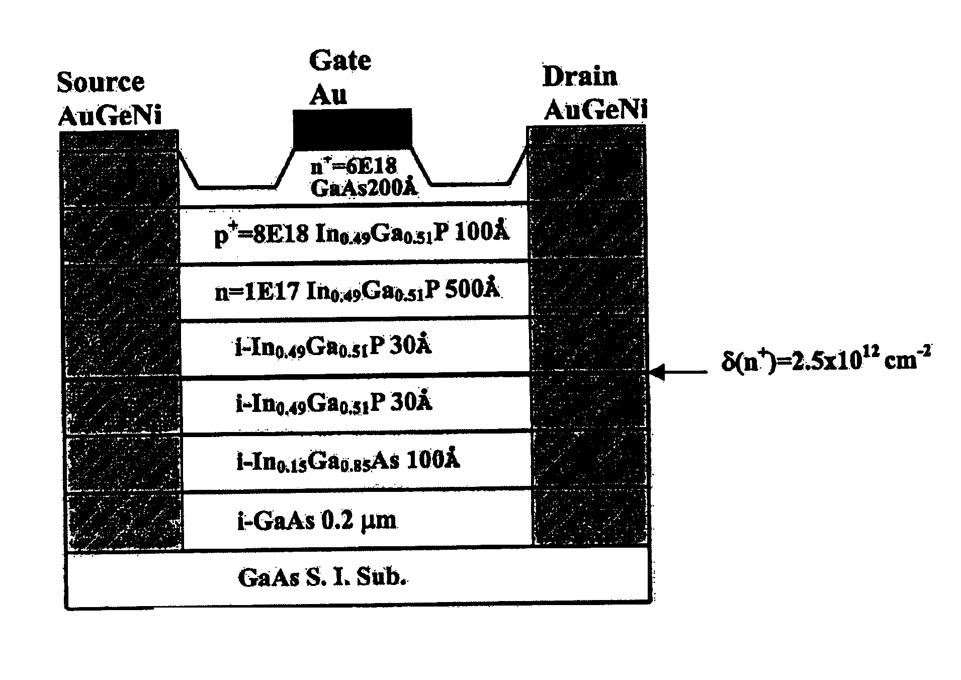
[0035]In this example, one InGaP / InGaAs / GaAs single δ-doped pHEMT device is proposed. As shown in FIG. 3, from bottom to up, its structure consists of one semi-insulating GaAs substrate on the basis, one 0.2 μm non-doped GaAs buffer layer over one semi-insulating GaAs substrate, one 100 Å non-doped In0.15Ga0.85As strain layer, one 30 Å non-doped In0.49Ga0.51P first spacer layer, one δ-doped carrier supplying layer with concentration of δ(n)=2.5×1012 cm−3, one 30 Å non-doped In0.49Ga0.51P second spacer layer, one 500 Å n-doped In0.49Ga0.51P layer with concentration of n=1×1017 cm−3, one 100 Å p+-doped In0.49Ga0.51P layer with concentration of p+=8×1018 cm−3, and one 200 Å n+-doped GaAs covering layer with concentration of n+=6×1018 cm−3. The metal Au of the gate electrode constitutes the ohmic contact over the covering layer. The metal AuGeNi of the drain electrode and source electrode lying beside the metal Au of the gate electrode respectively both constitute the ohmic contact over...

example 2

[0037]As shown in FIG. 9, this example presents InGaP / InGaAs / GaAs double δ-doped pHEMT device, whose structure is similar to Example 1. In the structure of this example, another carrier supplying layer, δ(n+), and another i-GaAs lay as an additional non-doped spacer layer are formed between the non-doped spacer layer, i-GaAs, and the InGaAs strain layer. The energy-band plot of the conduction band of the device is illustrated as FIG. 10. There are two 2DEG forming in the InGaAs strain layer. Because the structure is double δ(n+)-doped, the concentration of the channel is so high that the threshold voltage will also increase. The two-terminal current-voltage output characteristic of double δ-doped pHEMT is shown as FIG. 11. The gate-drain breakdown voltage is over 8 V, and the forward turn-on voltage is 1.7 V. Compared with single δ-doped pHEMT device, the forward turn-on voltage of double δ-doped pHEMT device is almost identical to that of single δ-doped pHEMT device because of the ...


PUM


Abstract

New pseudomorphic high electron mobility transistors (pHEMT's) with extremely high device linearity having an n+ / p+ / n camel-gate heterostructure and δ-doped sheet structure is disclosed. For the example of InGaP / InGaAs / GaAs δ-doped pHEMT's with an n+-GaAs / p+-InGaP / n-InGaP camel-gate structure, due to the p-n depletion from p+-InGaP gate to channel region and the presence of large conduction band discontinuity (ΔEc) at InGaP / InGaAs heterostructure, the turn-on voltage of gate is larger than 1.7 V. Attributed to the applied gate voltage partly lying on the camel gate and influence of the carrier modulation, the change of total depletion thickness under gate bias is relatively small, and high drain current and linear transconductance can be achieved, simultaneously. The excellent device performances provide a promise for linear and large signal amplifiers and high-frequency circuit applications.

Description

FIELD OF THE INVENTION[0001]This invention is related to a pseudomorphic High Electron Mobility Transistors (pHEMT's), which has an n+ / p+ / n heterostructure camel-gate and a δ-doped layer structure.BACKGROUND OF THE INVENTION[0002]Recently, devices made of compound semiconductor material for high-speed, microwave, and power circuit applications have attracted a great deal of attention and played an important role in electronic integrated circuit field. As far as Field Effect Transistor (FET) is concerned, in order to make the devices operate at high frequency, reducing the FET gate's length, raising the carrier mobility, and decreasing the transport time are necessary. All kinds of high-performance devices, such as Metal Semiconductor Field Effect Transistor (MESFET), High Electron Mobility Transistor (HEMT), Doped Channel Field Effect Transistor (DCFET), and δ-doped layer Field Effect Transistor (δ-doped FET), have been successfully developed and widely applied to digital and microw...

Claims


Application Information

Patent Timeline
Patent Type & Authority Patents(United States)
IPC IPC(8): H01L29/66H01L29/772H01L31/0264H01L31/0328H01L33/00H01L29/778
CPCH01L29/7784
Inventor TSAI, JUNG-HUI
Owner NAT KAOHSIUNG NORMAL UNIV
Why Eureka
Try Eureka