High-gain photodetector with separated PN junction and rare earth doped region and a method of forming the same

Inactive Publication Date: 2005-09-13
STMICROELECTRONICS SRL
View PDF3 Cites 17 Cited by
  • Summary
  • Abstract
  • Description
  • Claims
  • Application Information

AI Technical Summary

Benefits of technology

[0012]The aim of the present invention is to provide an improved photodetector which is able to detect light at preset frequencies and which moreover has high detection efficiency. According to the present invention there are provided a photodetector of semiconductor material and a manufacturing process thereof. Aspects include a photodetector comprising a semiconductor material body housing a PN junction and a sensitive

Problems solved by technology

However, in these cells the conversion efficiency is very low, of abou

Method used


Image

  • High-gain photodetector with separated PN junction and rare earth doped region and a method of forming the same
  • High-gain photodetector with separated PN junction and rare earth doped region and a method of forming the same
  • High-gain photodetector with separated PN junction and rare earth doped region and a method of forming the same

Examples


Embodiment Construction

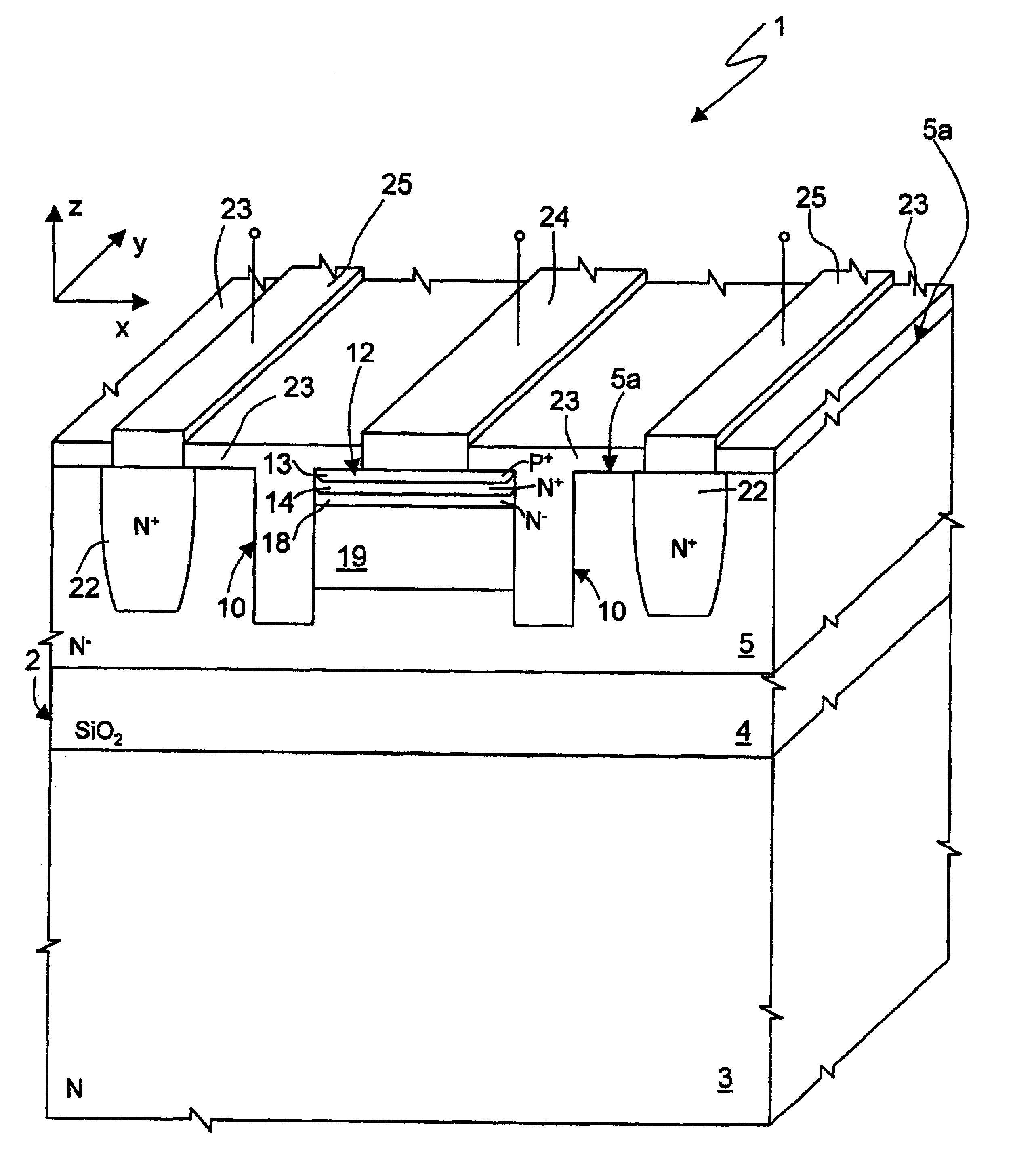
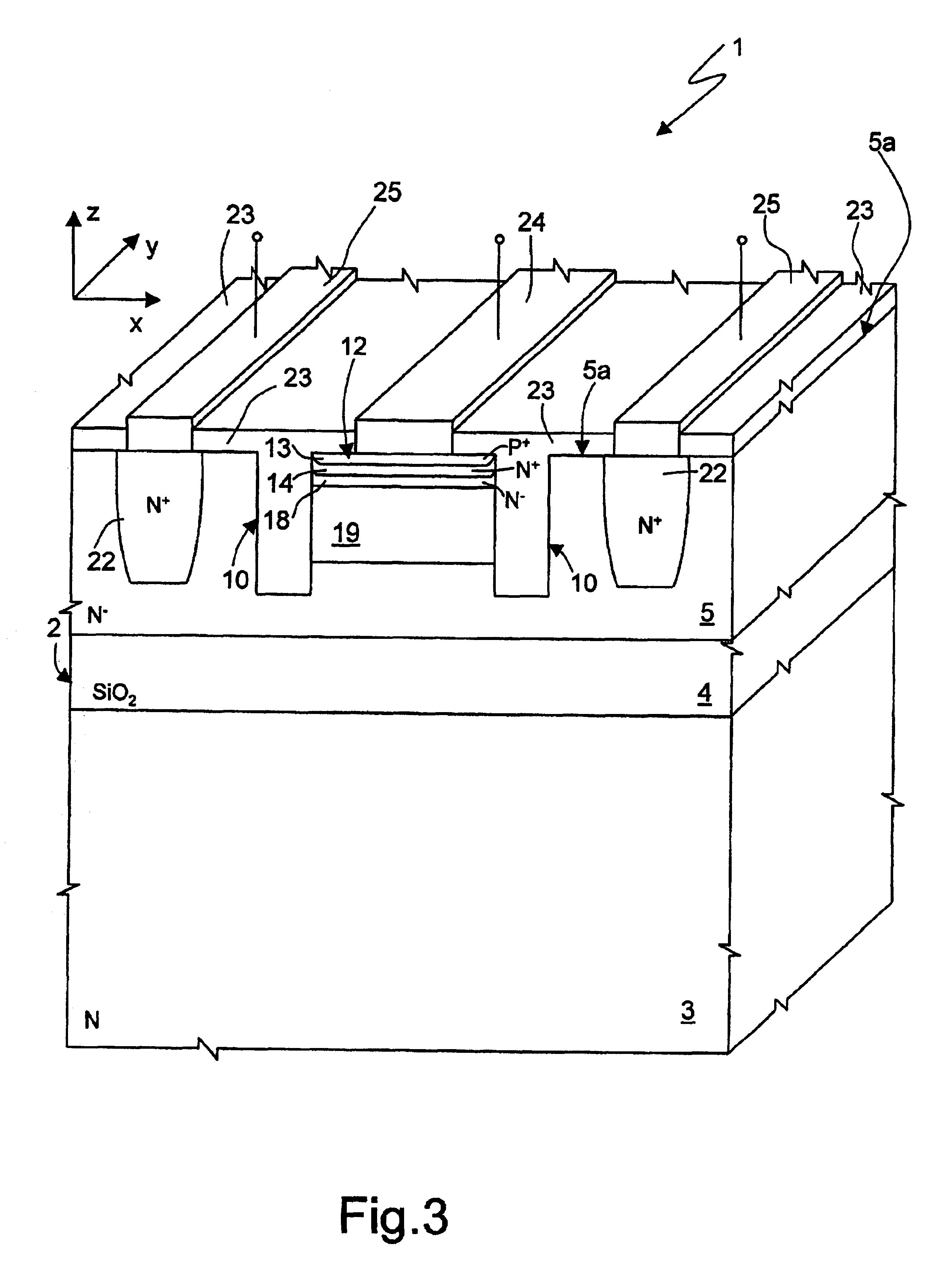
[0024]FIG. 3 shows a cross-section of a portion of an integrated device housing a photodetector according to the invention.

[0025]In particular, as shown in FIG. 3, the photodetector, designated by 1, is formed in a silicon-on-insulator (SOI) substrate 2 including a first monocrystalline region 3 of N-type, an oxide region 4, and a second monocrystalline region 5 of N−-type, which has a top surface 5a.

[0026]Two trenches 10 extend inside the second monocrystalline region 5 and delimit laterally between them and active region 12 of the photodetector. The active region 12 comprises a surface region 13 of P+-type facing the top surface 5a of the second monocrystalline region 5; a junction region 14 of N+-type arranged directly beneath, and contiguous to, the surface region 13; a separation region 18 formed by the second monocrystalline region 5, and thus of the N−-type; and a sensitive region 19, doped with a rare earth, for example erbium (Er), holmium (Ho), neodymium (Nd), or promethi...


PUM


Abstract

The high-gain photodetector is formed in a semiconductor-material body which houses a PN junction and a sensitive region that is doped with rare earths, for example erbium. The PN junction forms an acceleration and gain region separate from the sensitive region. The PN junction is reverse-biased and generates an extensive depletion region accommodating the sensitive region. Thereby, the incident photon having a frequency equal to the absorption frequency of the used rare earth crosses the PN junction, which is transparent to light, can be captured by an erbium ion in the sensitive region, so as to generate a primary electron, which is accelerated towards the PN junction by the electric field present, and can, in turn, generate secondary electrons by impact, according to an avalanche process. Thereby, a single photon can give rise to a cascade of electrons, thus considerably increasing detection efficiency.

Description

BACKGROUND OF THE INVENTION[0001]1. Field of the Invention[0002]The present invention relates to a high-gain photodetector of semiconductor material and to a manufacturing process thereof.[0003]2. Description of the Related Art[0004]As is known, silicon is currently the main material used for manufacturing integrated electronic components and it is used for implementing a large variety of electrical functions.[0005]At present, a new optical-communication technology is emerging wherein the elementary information is carried by optical signals. Wavelengths for optical communications are in the 1.3 to 1.55 μm range. It is moreover desirable to combine optical and electronic functions in a single silicon device, by combining electronic technologies and optical technologies.[0006]High-internal-gain detectors are required for different applications, such as single-photon counting and quantum computing. Avalanche photodetectors (APDs) with internal gain up to 105 are particularly suitable f...

Claims


Application Information

Patent Timeline
IPC IPC(8): H01L31/102H01L31/0264H01L31/0288H01L31/107
CPCH01L31/0288H01L31/107Y02B10/10Y02E10/50
Inventor COFFA, SALVATORELIBERTINO, SEBANIAFRISINA, FERRUCCIO
Owner STMICROELECTRONICS SRL
Why Eureka
Try Eureka