High data rate write process for non-volatile flash memories

a write process and flash memory technology, applied in the direction of digital storage, electric analogue stores, instruments, etc., can solve the problems of high current drain, affect the accuracy and repeatability of write operations, etc., and achieve the effect of high data rate and less nois

Inactive Publication Date: 2005-09-13
INNOVATIVE MEMORY SYST INC
View PDF49 Cites 74 Cited by
  • Summary
  • Abstract
  • Description
  • Claims
  • Application Information

AI Technical Summary

Benefits of technology

[0009]In accordance with the invention, a non-volatile memory has multiple write pipelines that are sequentially started on programming operations and has a shared charge pump that supplies drain-to-source currents during the programming operations. With sequential starts, the programming operations are staggered, and the peak current for the multiple programming operations do not occur at the same time. Accordingly, sequential starting of programming operations in the write pipelines avoids the high combined peak current that occurs in memories that simultaneously start multiple programming operations. The staggered operations of the write pipelines also provide a high data rate because all of the write pipelines can operate at the same time to provide the same data rate as a conventional memory that performs parallel programming operations. The smaller peak current allows the charge pump and associated voltage regulation circuitry to be smaller than similar circuitry used in conventional memory that performs parallel programming operations. Additionally, since spikes in the current from the charge pump are relatively small, memories with sequential or staggered programming operations generate less noise in the supply voltage during programming, and permit accurate programming for applications such as analog or multiple-bits-per-cell storage.

Problems solved by technology

However, as noted above for programming operations, current drain is high at the beginning of the programming operation and falls as a memory cell threshold voltage rises.
Accordingly, the charge pumps and the supply voltage in the memory are subject to changing current demands which cause voltage fluctuations or noise that can affect the accuracy and repeatability of write operations.

Method used


Image

  • High data rate write process for non-volatile flash memories
  • High data rate write process for non-volatile flash memories
  • High data rate write process for non-volatile flash memories

Examples


Embodiment Construction

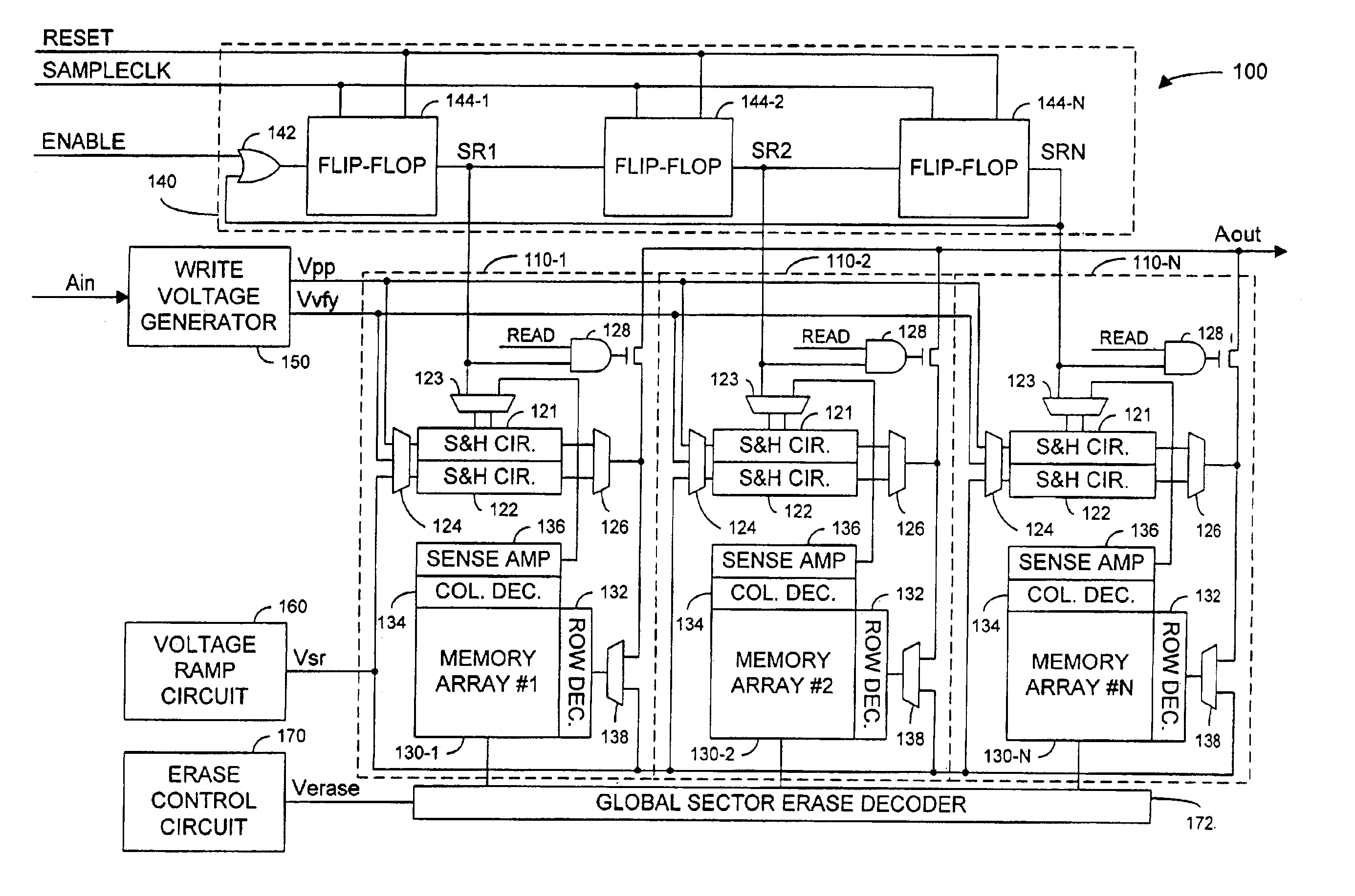
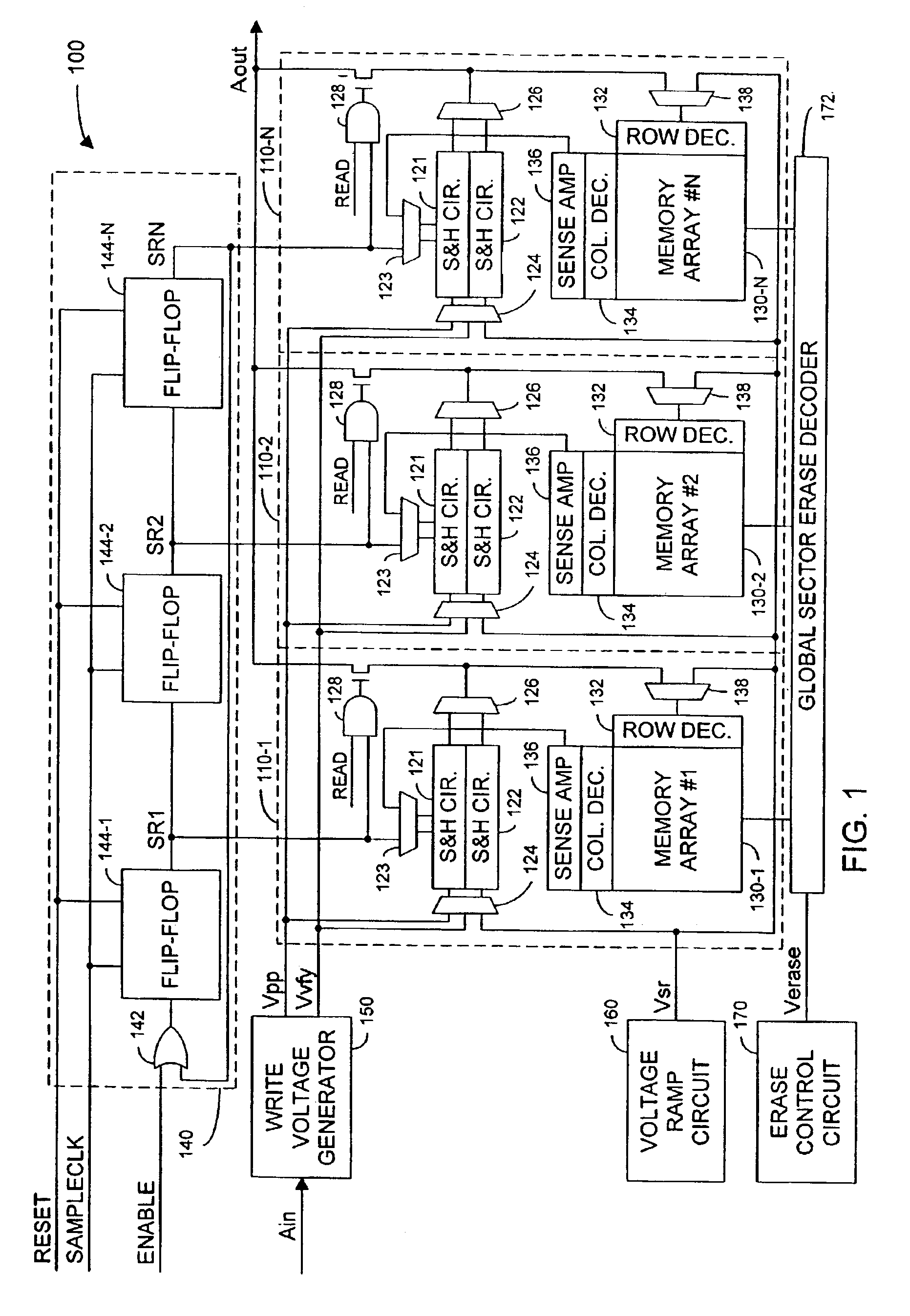
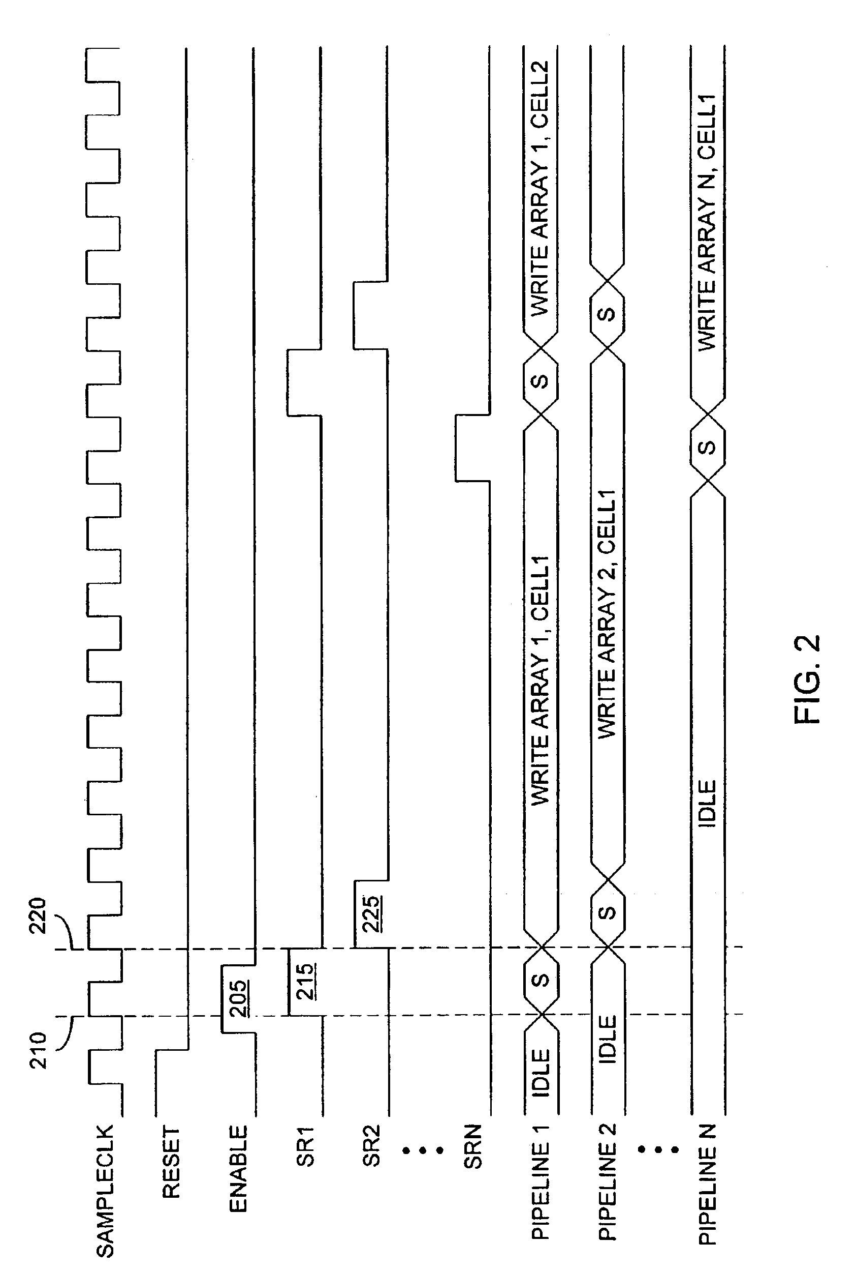
[0019]A non-volatile floating-gate memory in accordance with an embodiment of the invention performs pipelined writes that stagger the starts of channel hot electron injection processes. The pipelined writes provide a high data rate by programming multiple memory cells at a time. However, the programming operations do not start or end simultaneously and are at different stages of completion. In accordance with an aspect of the invention, a single charge pump supplies a high voltage that drives drain-to-source currents for programming processes such as channel hot electron injection in multiple memory cells. Since the programming operations have staggered starts, the maximum current that the charge pump must provide is less than the peak current for a single programming operation times the number of memory cells being simultaneously programmed. Accordingly, at a fixed data rate, the charge pump required for the pipelined write scheme can be smaller than the charge pump required for a...


PUM


Abstract

A non-volatile semiconductor memory includes: multiple write pipelines, each including a memory array; a timing circuit which sequentially starts programming operations in the pipelines; and a shared charge pump and voltage regulation circuit that drives a current through the memory cells being programmed. Staggering the starts of programming operations reduces the current demand on the charge pump because spikes that occur at the starts of programming operations, for example, when using channel hot electron injection, are distributed over time rather than occurring all at once. Noise, which can reduce the accuracy of write operations, is also reduced because the total current required from the charge pump is more nearly constant. As further aspect of the invention, each write pipeline can perform a write operation as alternating programming cycles and verify cycles. During a programming cycle, the shared charge pump drives a current through a selected memory cell to change the threshold voltage of the selected memory cell. During a verify cycle, the write circuit determines whether the selected memory cell has reached its target threshold voltage level. The write pipelines can be partitioned into two banks where pipelines in one bank perform programming cycles while pipelines in the other bank perform verify cycles. More generally the write pipelines are partitioned into multiple banks where each bank starts programming cycles at times that differ from the starts of programming cycles in the other banks.

Description

CROSS REFERENCE TO RELATED APPLICATION[0001]This patent document is a continuation of U.S. application Ser. No. 10 / 042,504, filed Oct. 18, 2001, now U.S. Pat. No. 6,606,267, which is a continuation U.S. application Ser. No. 09 / 670,764, filed Sep. 27, 2000, now U.S. Pat. No. 6,314,025, which is in turn a continuation of U.S. application Ser. No. 09 / 128,225, filed Aug. 3, 1998, now U.S. Pat. No. 6,134,145, which is a continuation-in-part of U.S. application Ser. No. 09 / 103,623, filed Jun. 23, 1998, now U.S. Pat. No. 5,969,986, which are all hereby incorporated by reference in their entirety.BACKGROUND[0002]1. Field of the Invention[0003]This invention relates to write processes for non-volatile memories and particularly to methods of reducing the current required when writing at a high data rate.[0004]2. Description of Related Art[0005]Semiconductor non-volatile memories such as EPROM, EEPROM, and flash memories, which permit electrical erasing and programming of memory cells, are wel...

Claims


Application Information

Patent Timeline
Patent Type & Authority Patents(United States)
IPC IPC(8): G11C11/56G11C16/10G11C7/10G11C16/26G11C16/06G11C27/00G11C11/34G11C16/12G11C16/34
CPCG11C7/1039G11C11/5621G11C11/5628G11C11/5642G11C16/10G11C16/12G11C16/26G11C16/3436G11C27/005G11C16/32G11C27/02
Inventor WONG, SAU C.
Owner INNOVATIVE MEMORY SYST INC
Why Eureka
Try Eureka